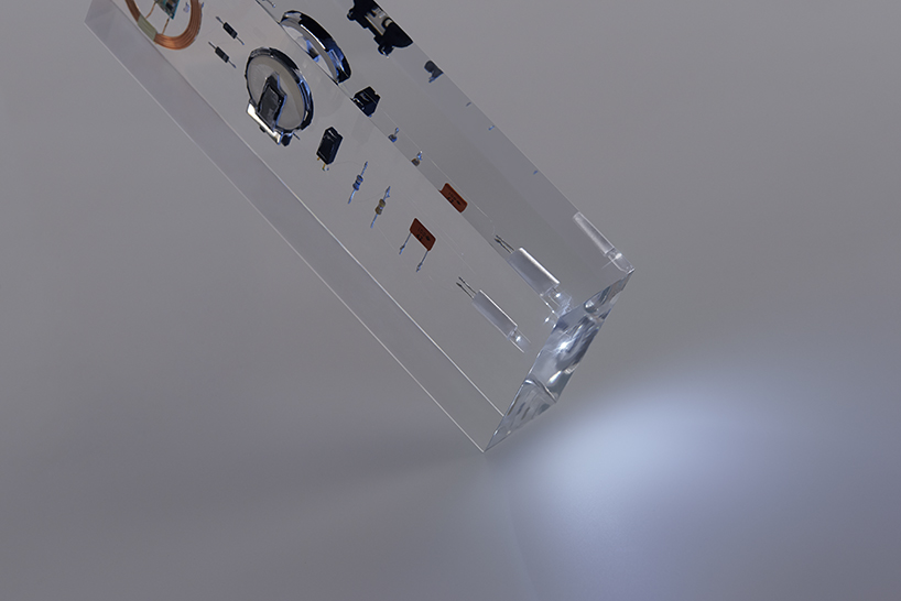
Transparency as material
How to Make Almost Anything Final projects
A: Making transparent PCBs
B: Ma-Um Objects: Ma-Um affordance as material
C : Wearable AR expirenece
[Outcome A: Making transparent PCBs]
*Shoutout to Wedyan - She helped me with everything from teaching how it works and doing the work of the etching part*
*Also thanks to Alan for listening carefully to my concept and connecting me with Wedyan*


[Original Proposal]
I want to make objects that don’t have ‘case’ and ‘electronic parts’ separated. I want to create objects that work as they are. For that, I will experiment with different materials to make PCBs. Eventually, like how we perceive clothes and shoes, our perception of tech devices will change as the novel material breaks the boundary between inside and outside. The dream is always high, but I would like to take the first step with this course.
[Related works]
https://www.taktproject.com/projects/composition-2/
Blurring the line of working part and viewing part - electric component and material


Below is an example in the book ‘Hertzian Tales’ by Dunne and Raby of how industrial design started to deal with the fluidity of electric technology

[Final Proposal]
Ever since the invention of the transistor, industrial designers' roles have changed from designing physical objects to designing packages of the electronics inside them. Industrial designers working on electronic devices become more like package designers working on cookie packages - almost nothing to do with the taste, form, or texture of the cookie itself, just making packages to contain the cookies.

The first transistor ever made, built by John Bardeen, William Shockley and Walter H. Brattain of Bell Labs in 1947. Original exhibited in Bell Laboratories.
[Process]
[Demo from Wedyan]


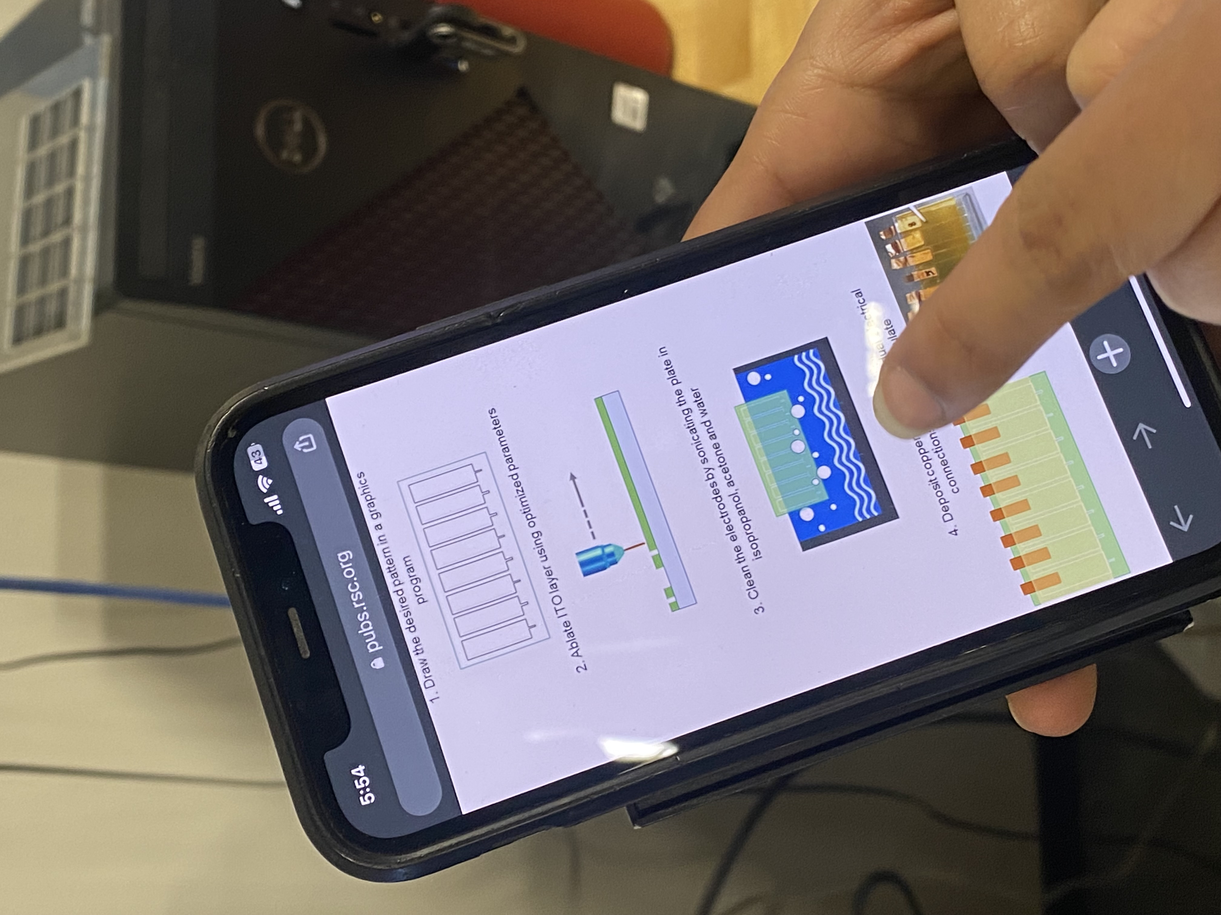
and We found this article - and it explains how to fabricate circuits outof ITO coated glasses with a regualr CO2 Laser cutter.

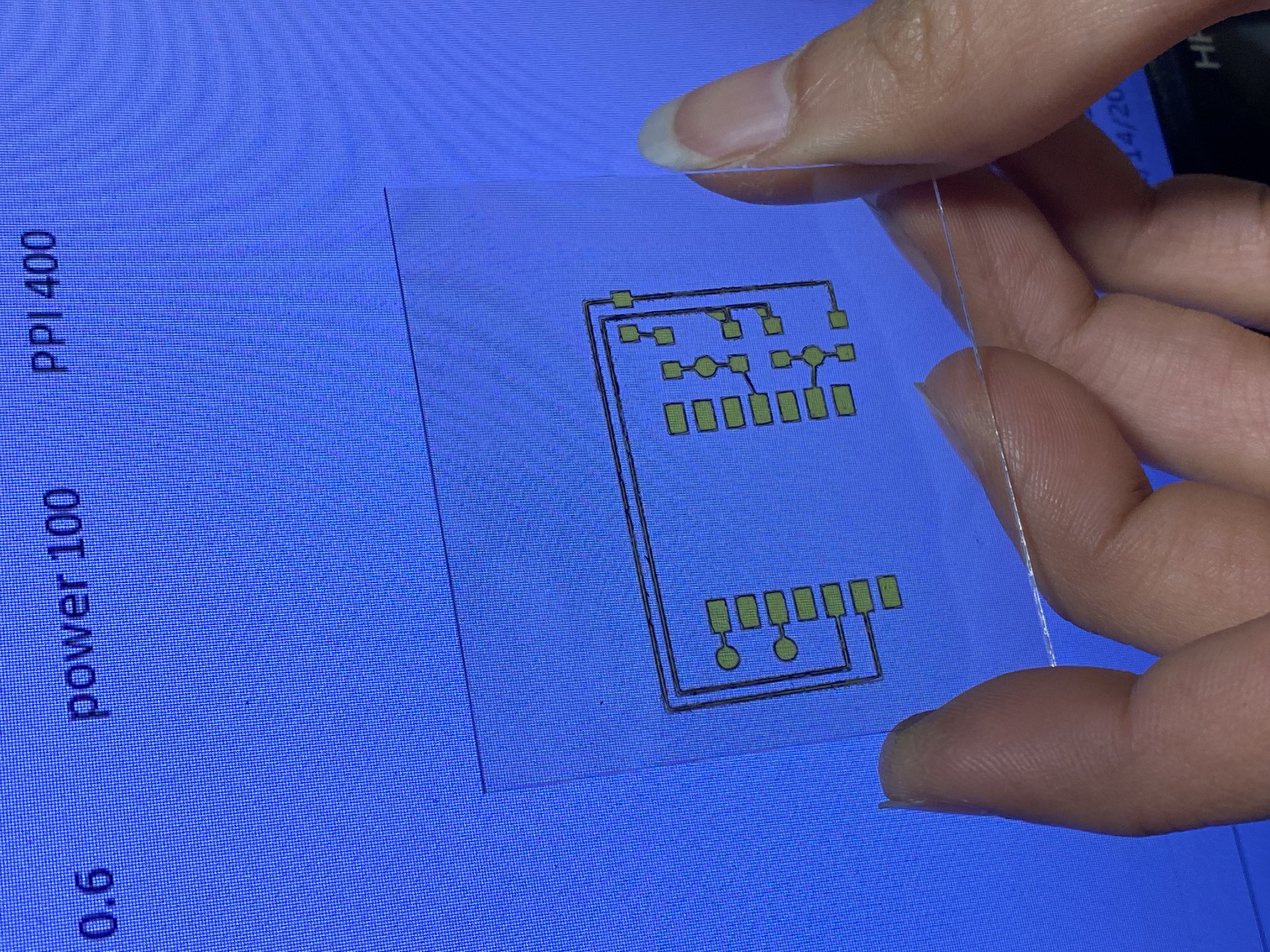
Cube prototype working as capacitive sensor
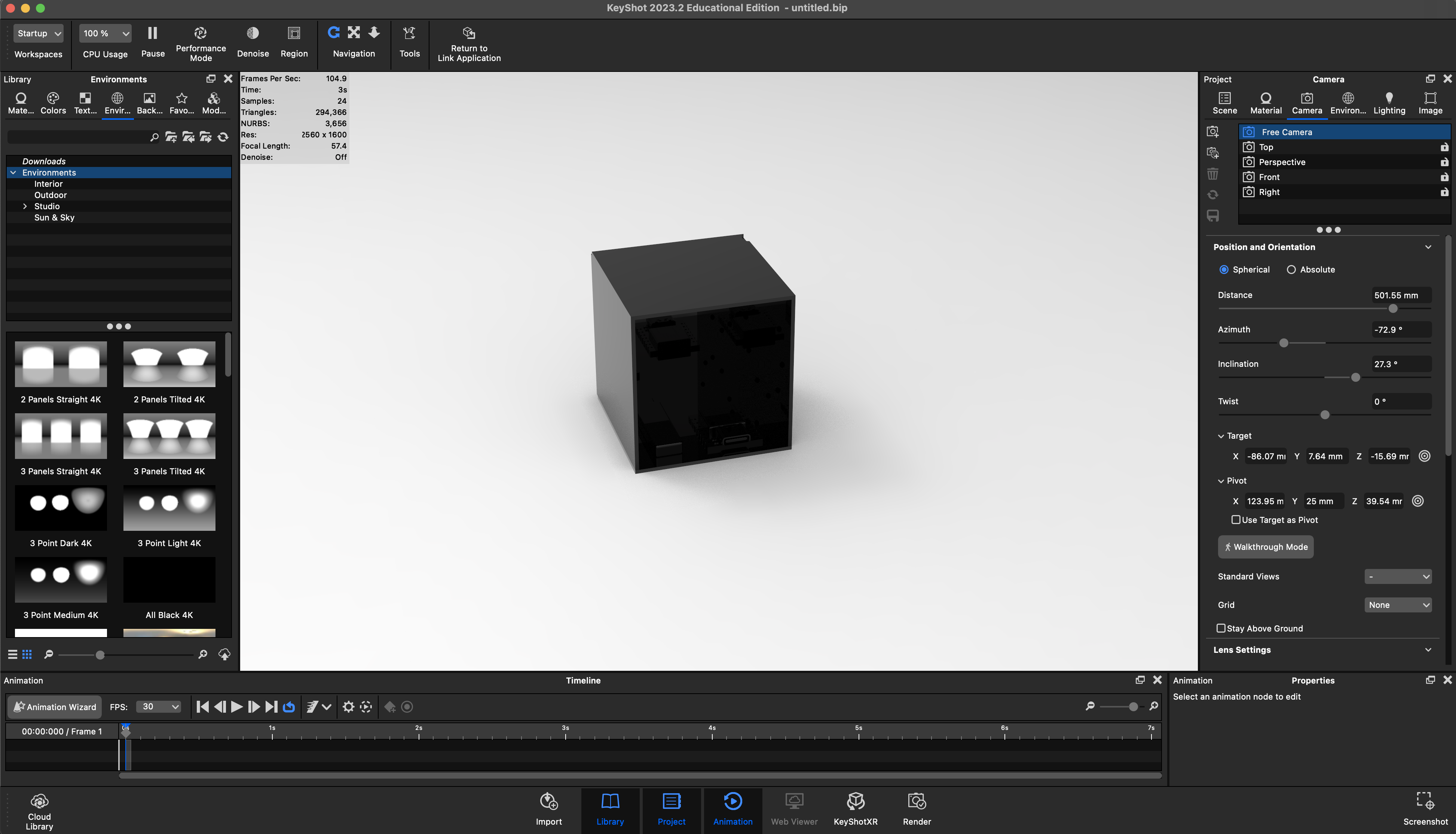
[Design]
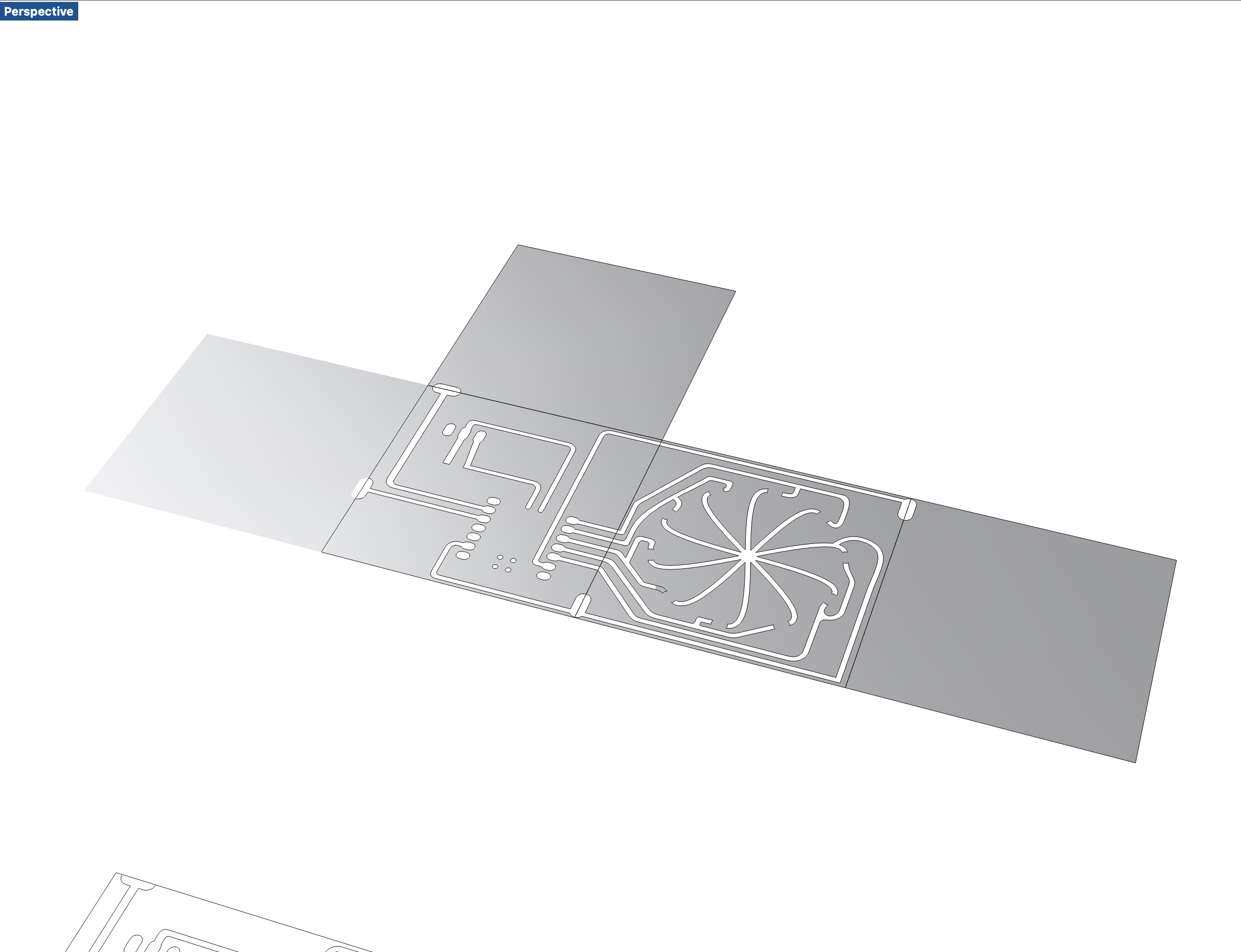
Designing a ‘Printed Circuit Box’, not a ‘Printed Circuit Board’One side had to be open for xiao board access, and the other three worked as capacitive sensing pads. One works as a base connection for xiao, and also routes for capacitive sensing are there. The last panel consists of 10 LEDs, perceivable from both sides of the glass.
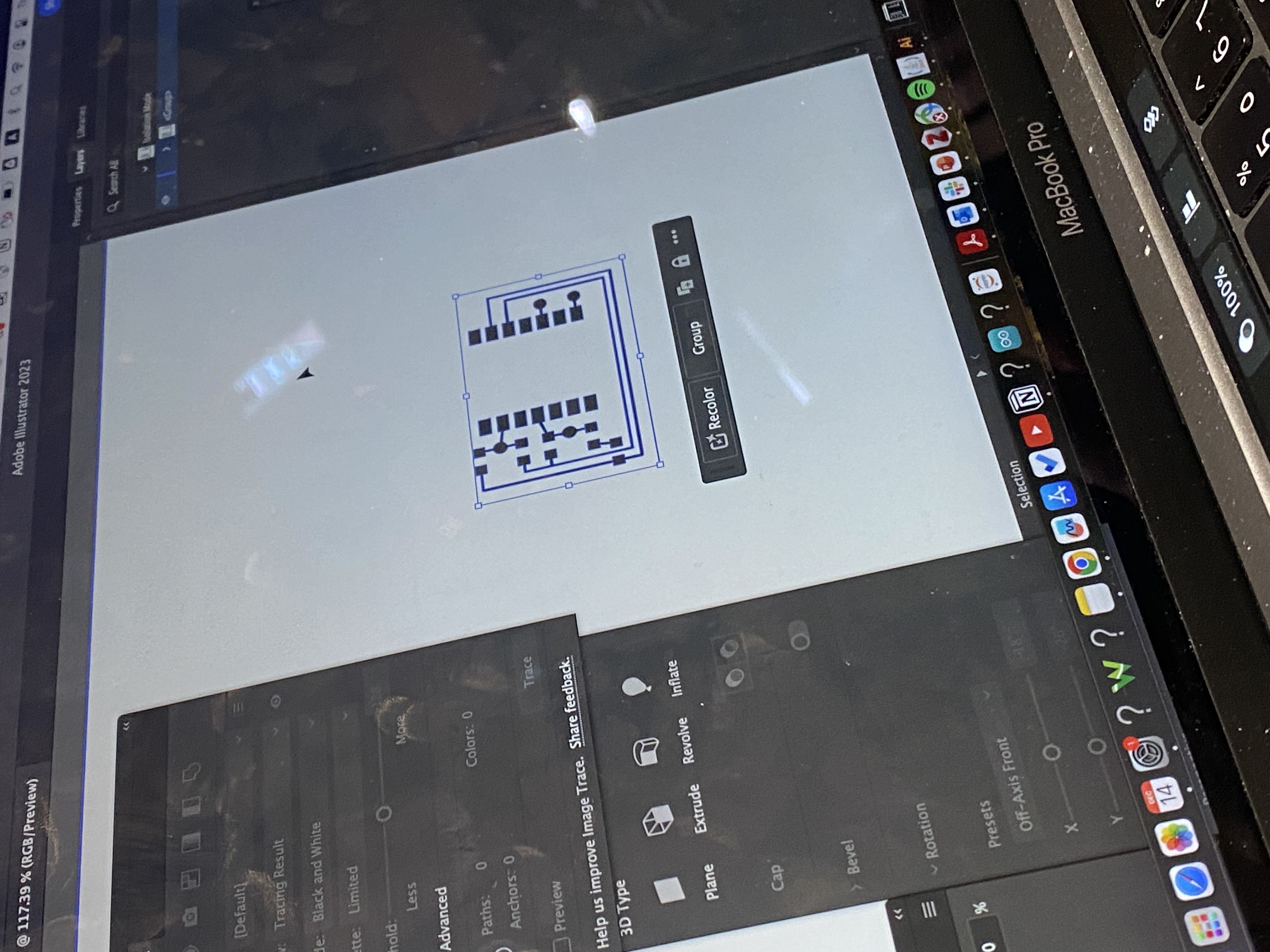
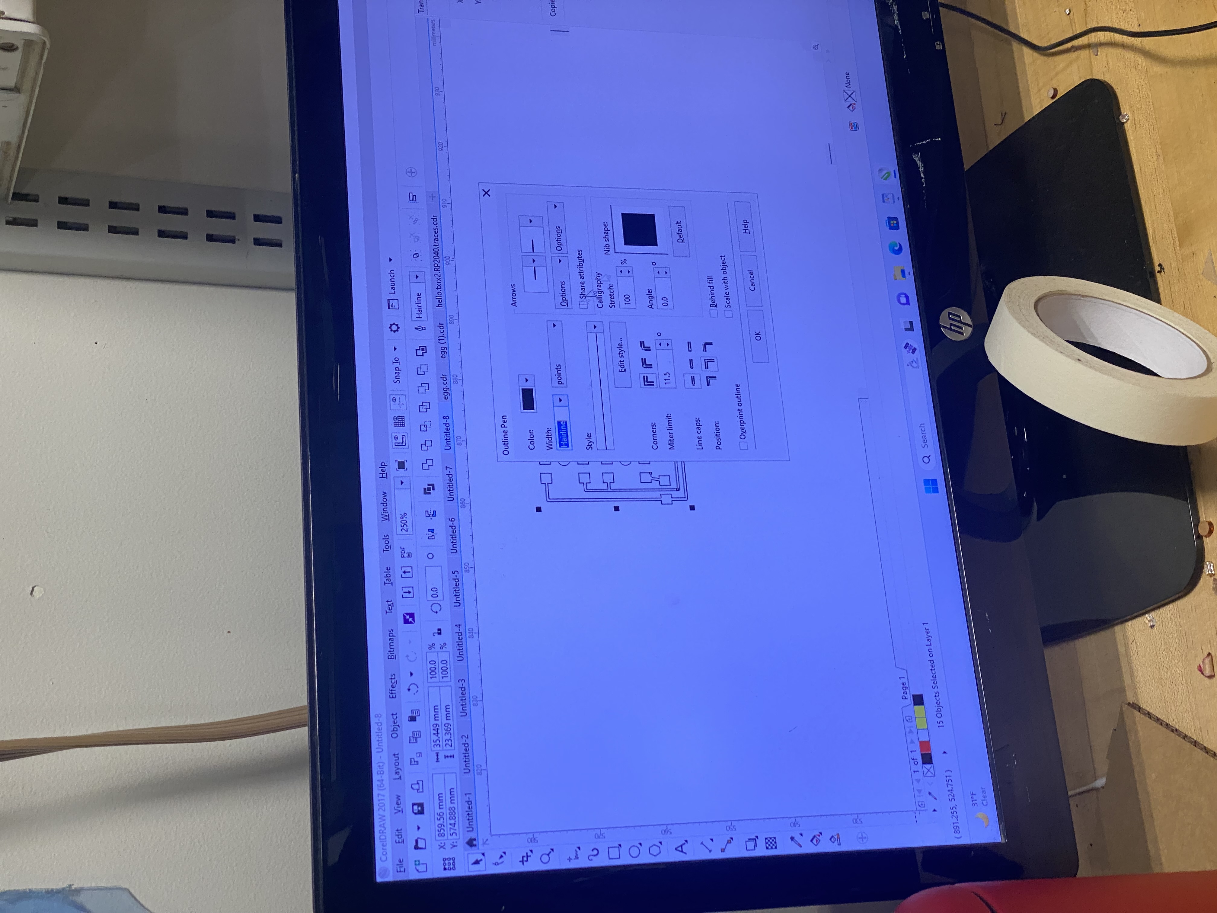
[Using Kicad]
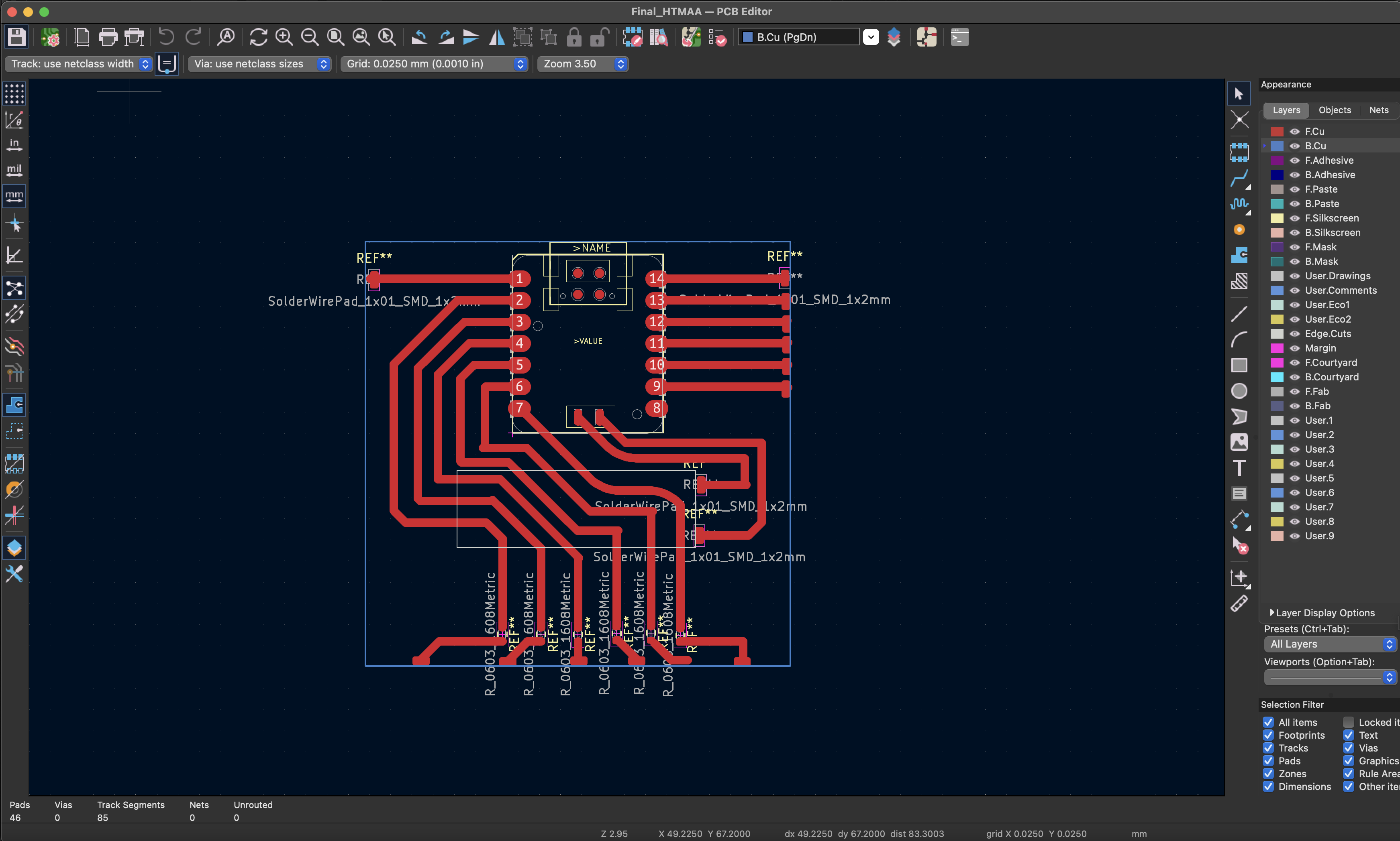
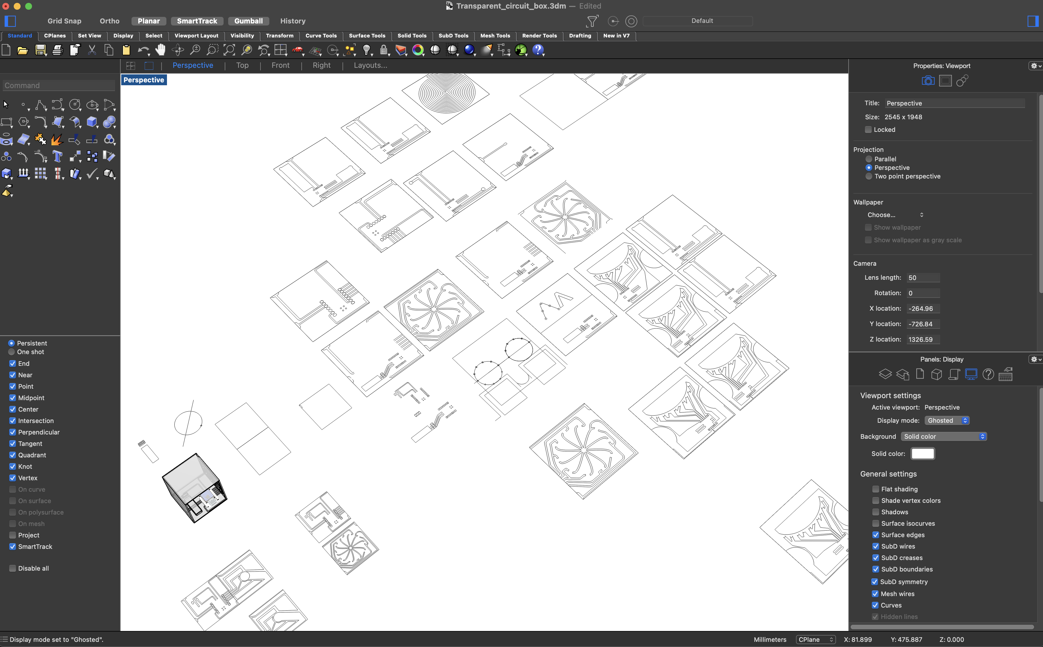
Needed more delicate control of the shape of routes -> decided to use Rhino3D
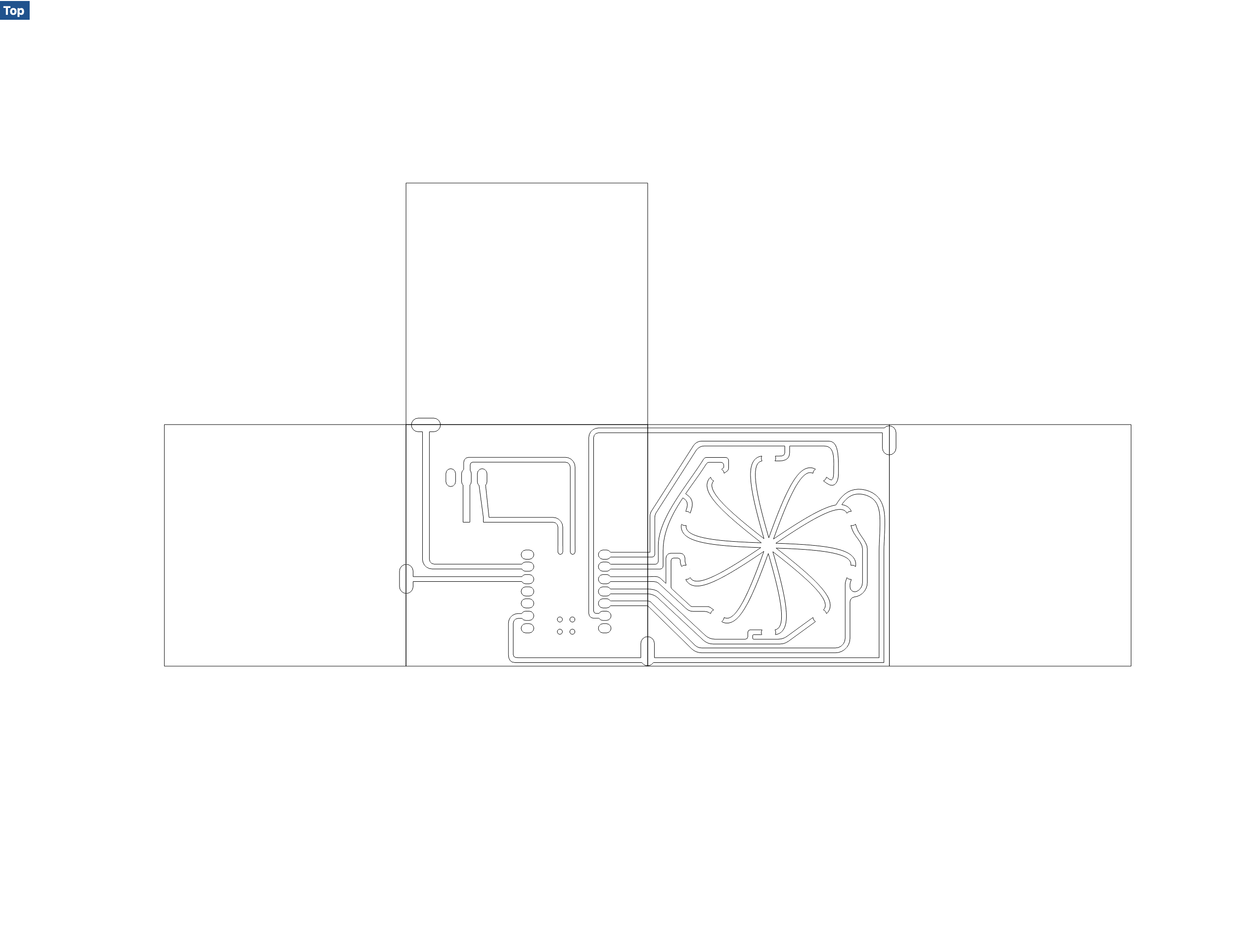
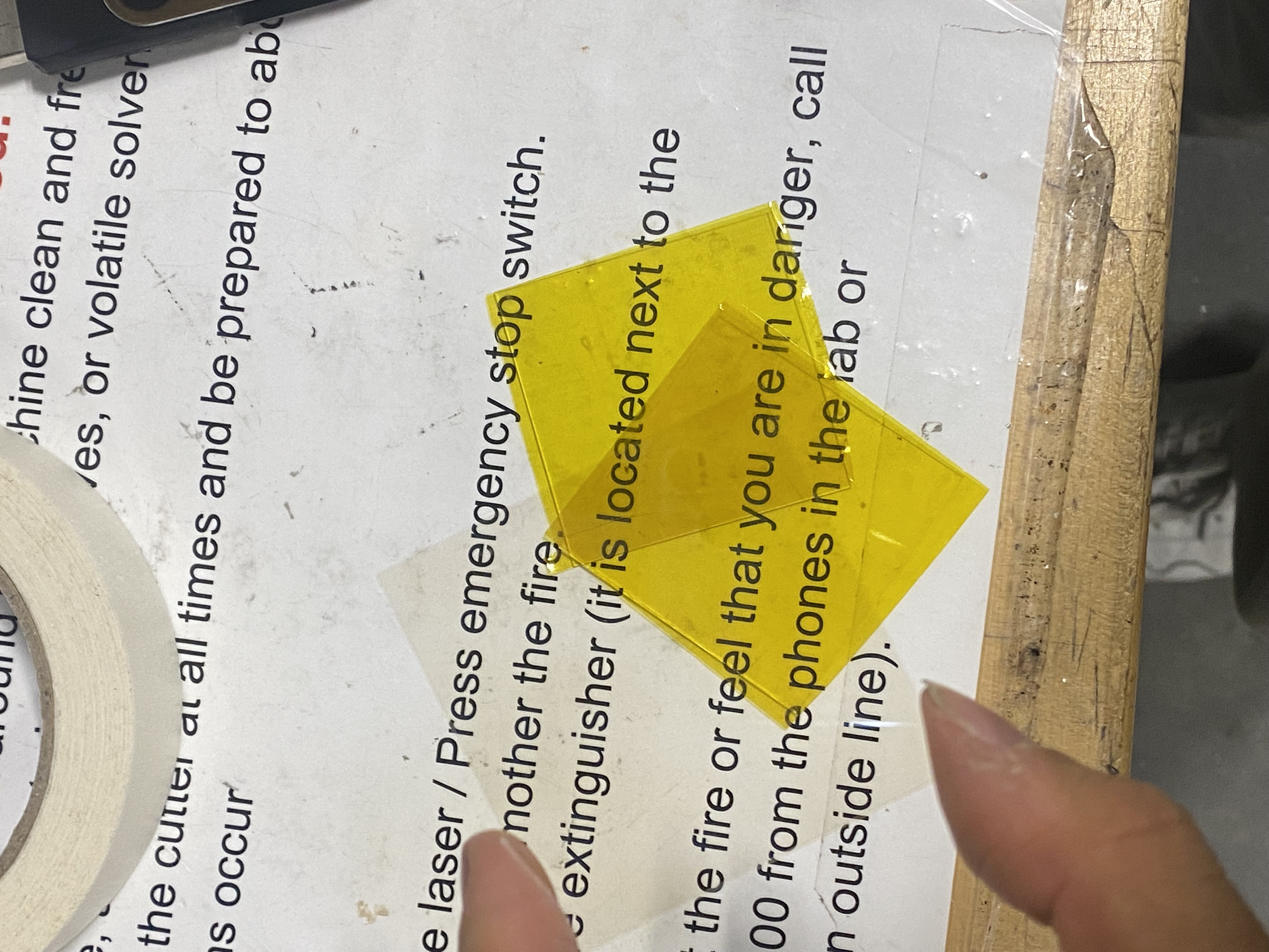
2D Flat layout - Does it look too decorative? They will be clear so it doesn’t matter.
Making surfaces out of the lines

Surfaces connected as a cube
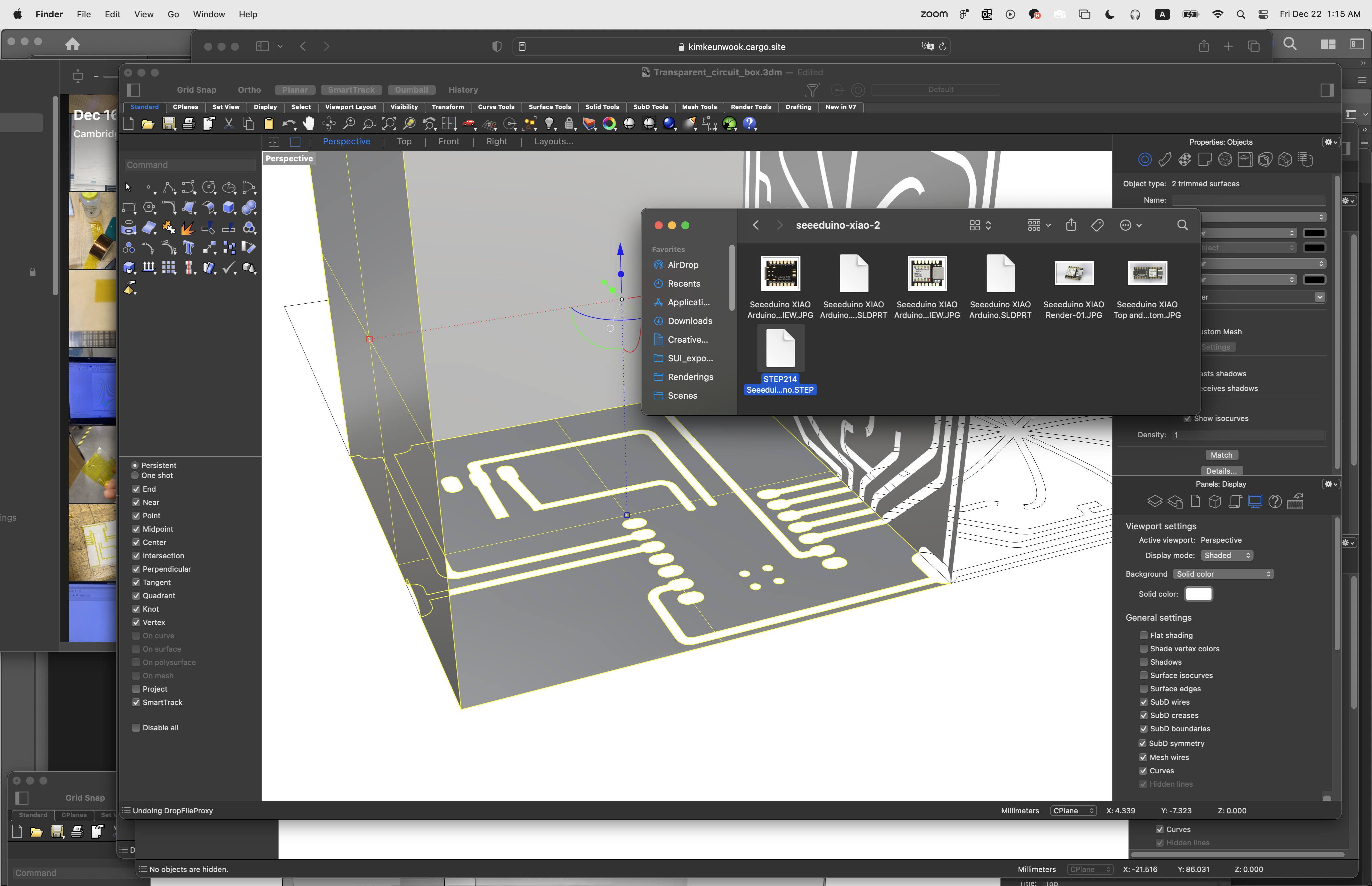
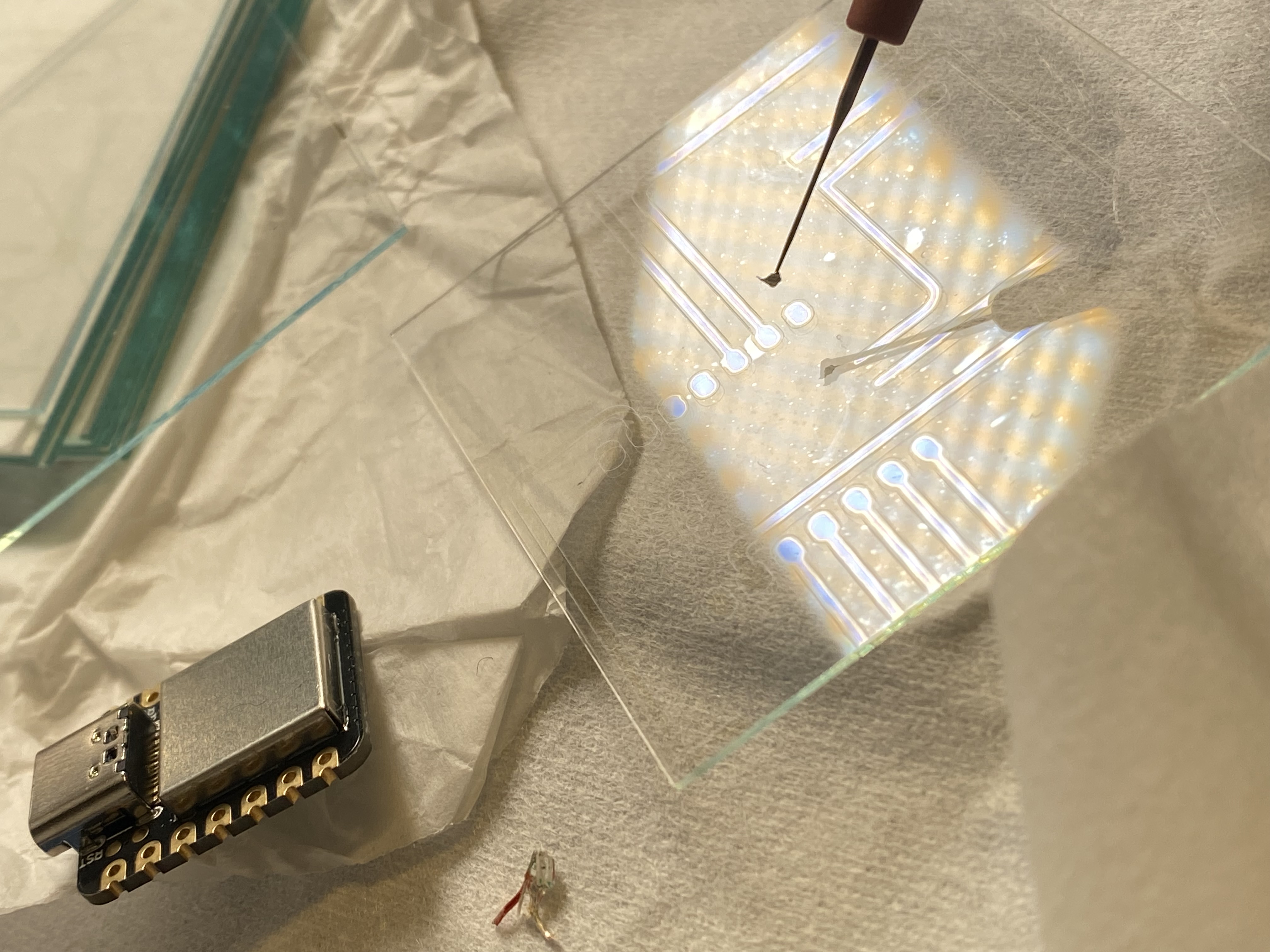
importing Xiao STEP model

‘Insert’ the model

Adjust the orientation

Finished 3D layout

Adding battery and switch - all measured with calipers

Adding LEDs
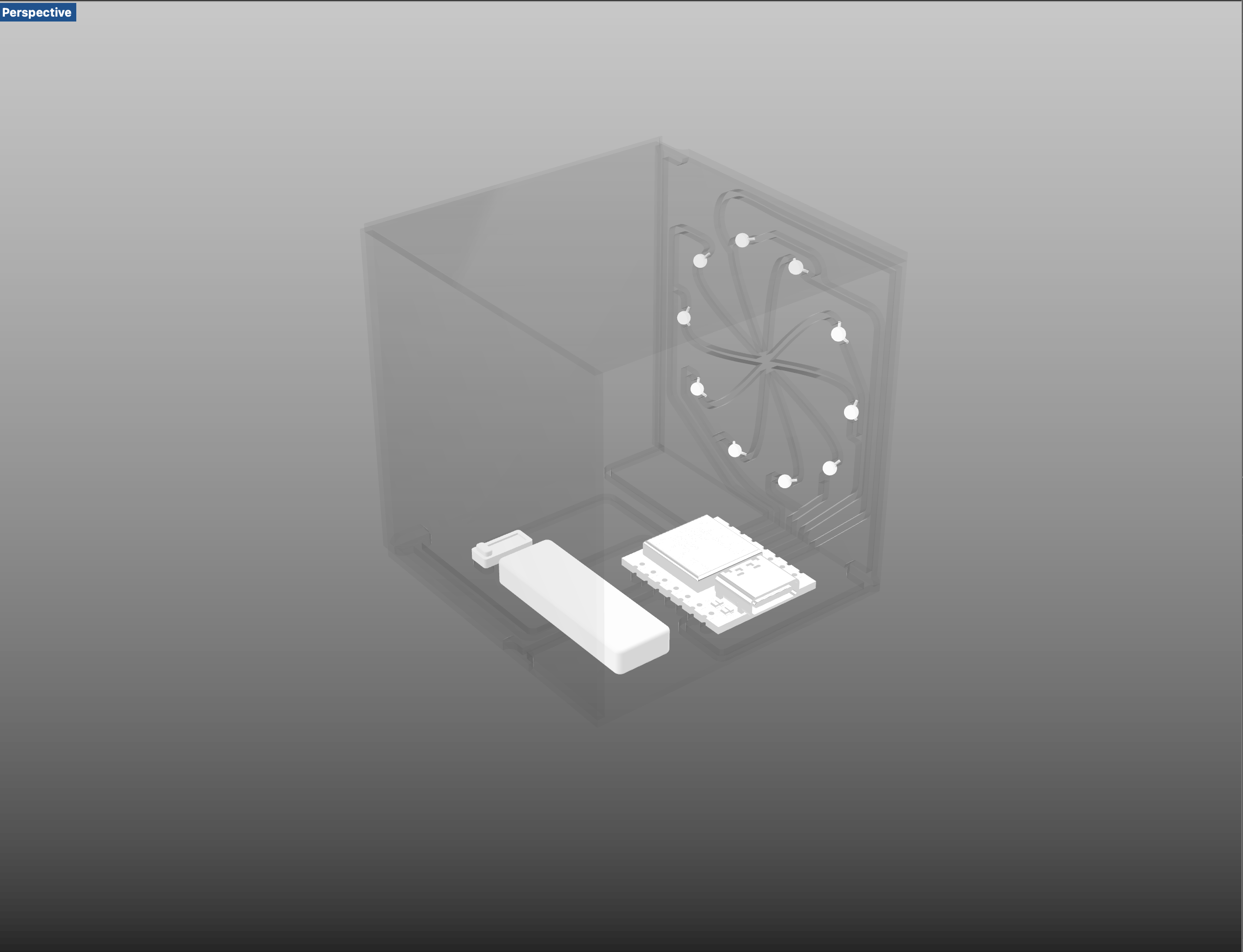

Renders in Rhino are not really recommendable - moving on to Keyshot for a better visualization
[Visualization]
[Outcome]
[Render Process - Keyshot]
Import the Rhino model directly using Rhino-Keyshot plugin. As the material is not assigned, everything is black or white or other colors based on the rhino render material setting.

Change the material from plastic to glass(solid)

Adding color with the ‘gem’ material - depending on the actual material properties, other materials can be applied.
When you import a STEP file or Solidworks file in Rhino, it’s unlikely they are divided into layers by material. The materials should be unliked first to be assigend for right ones.

You can set the right material to the model after several commands such as Ungroup / Explode / assigning material
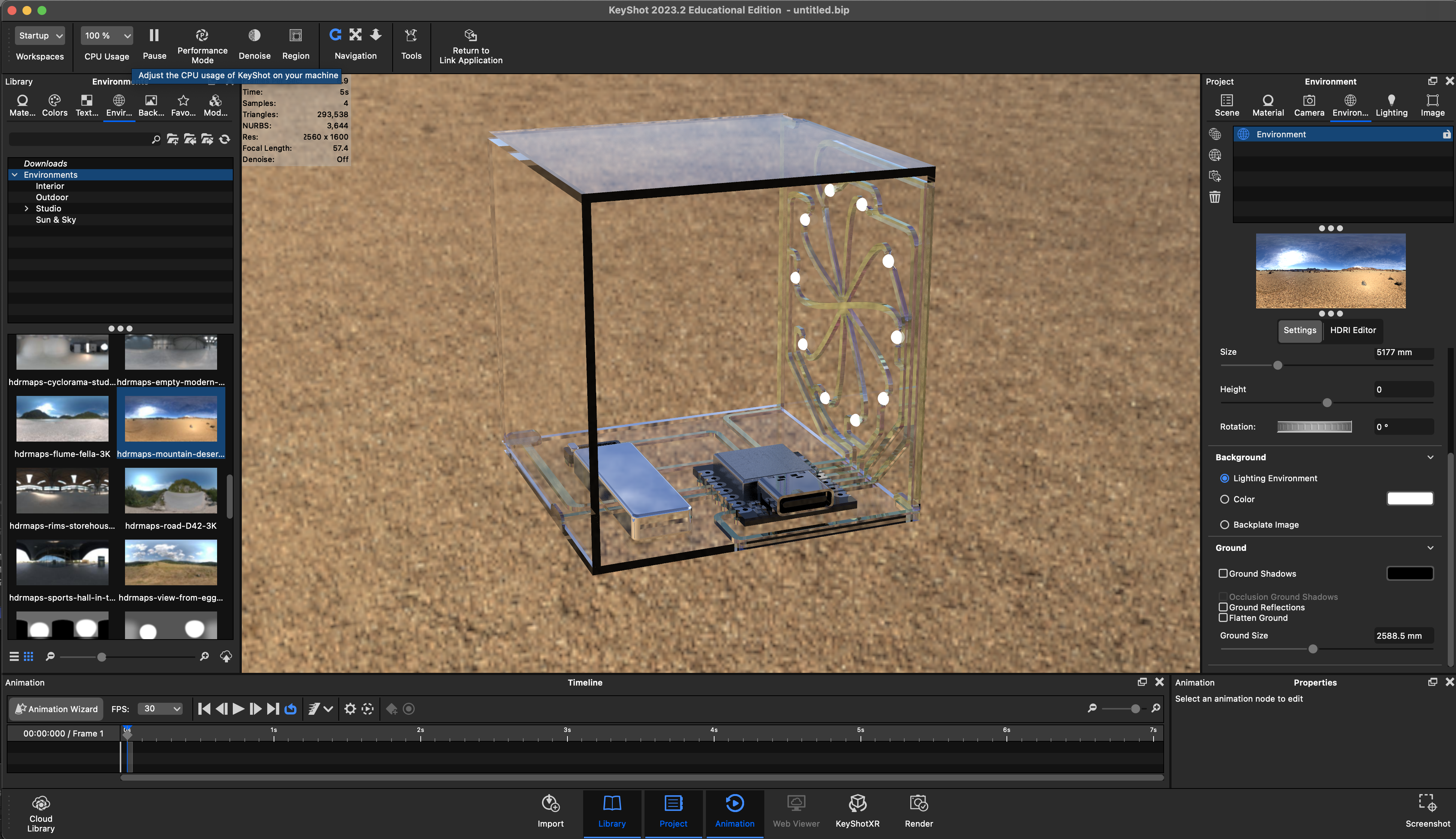
For clear / transparent material, the reflection, texture, and what is behind the object matter.
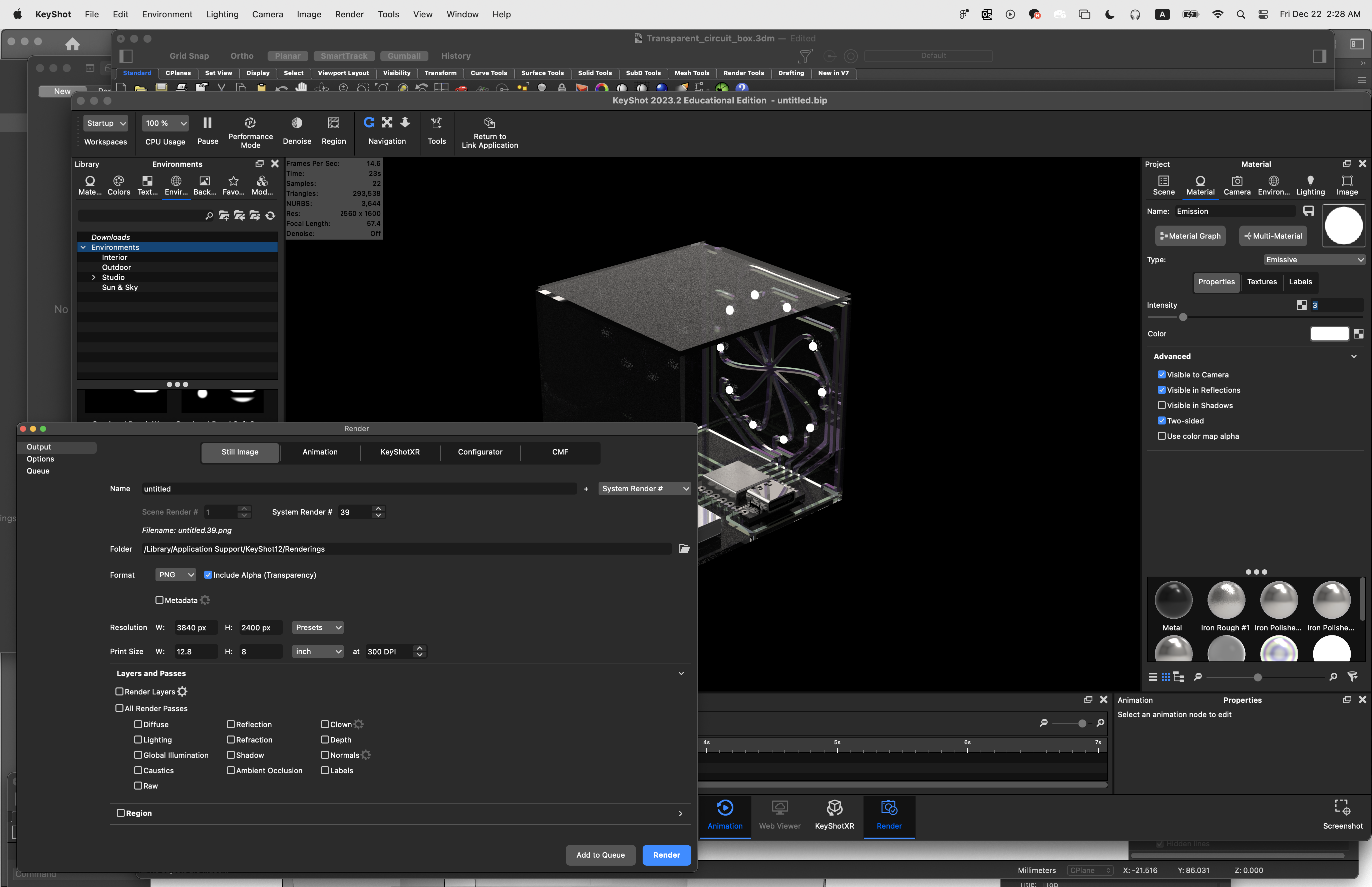
FInally, after assigning lights with emissive and changing the background color, render the final image.
[Process - CAD]
Hundreds of iterations are inevitable to make a working prototype
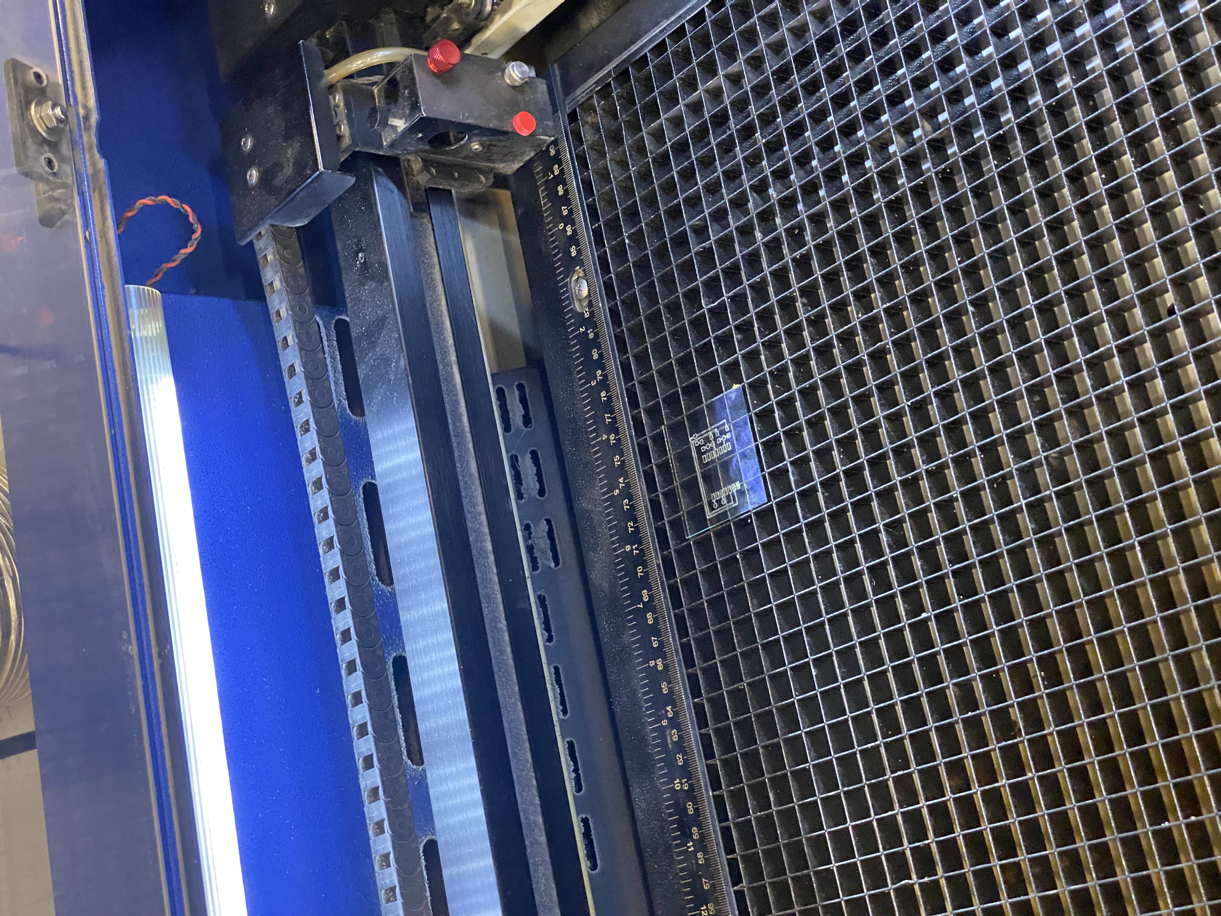
[Prototype Production]

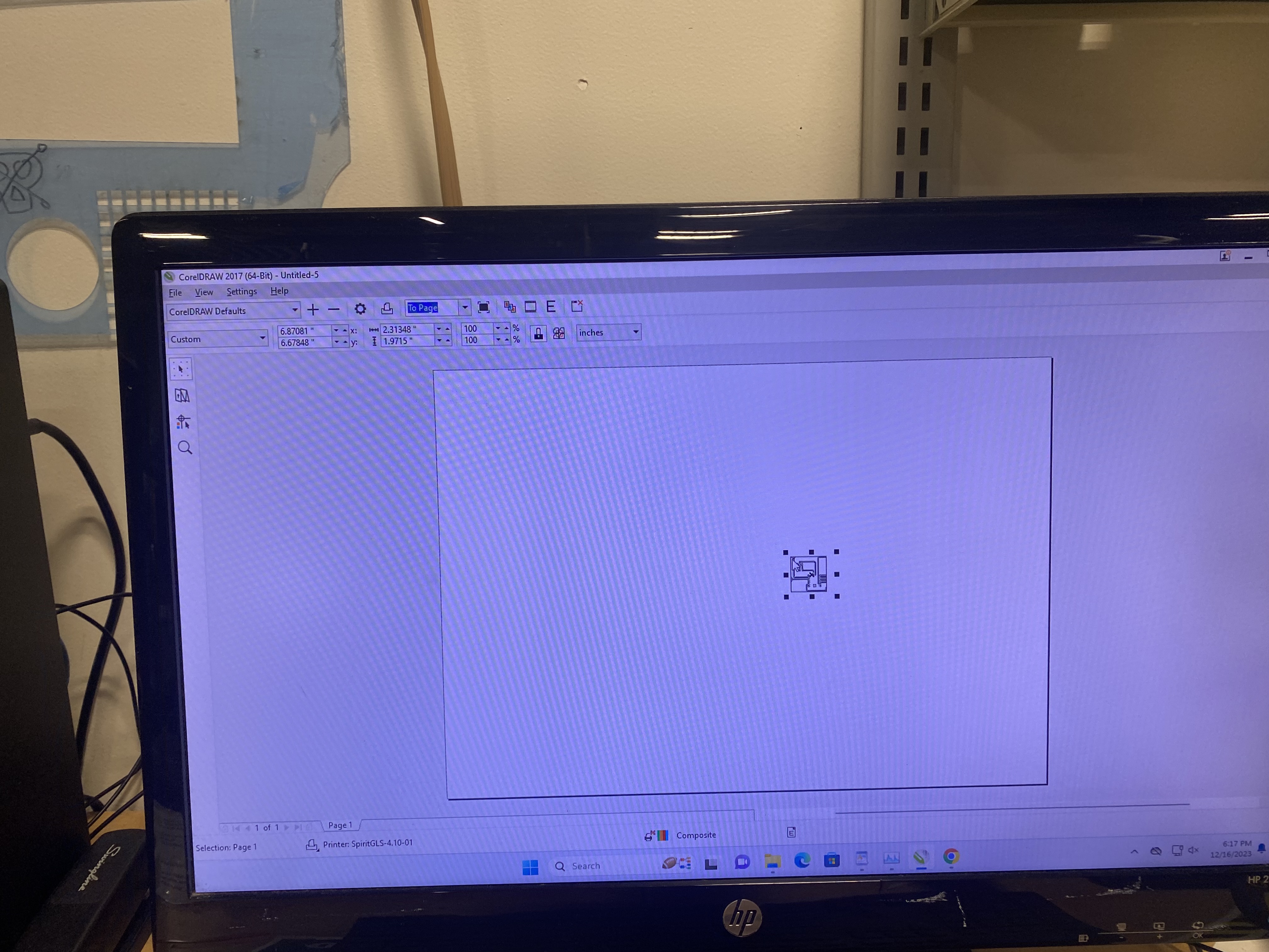
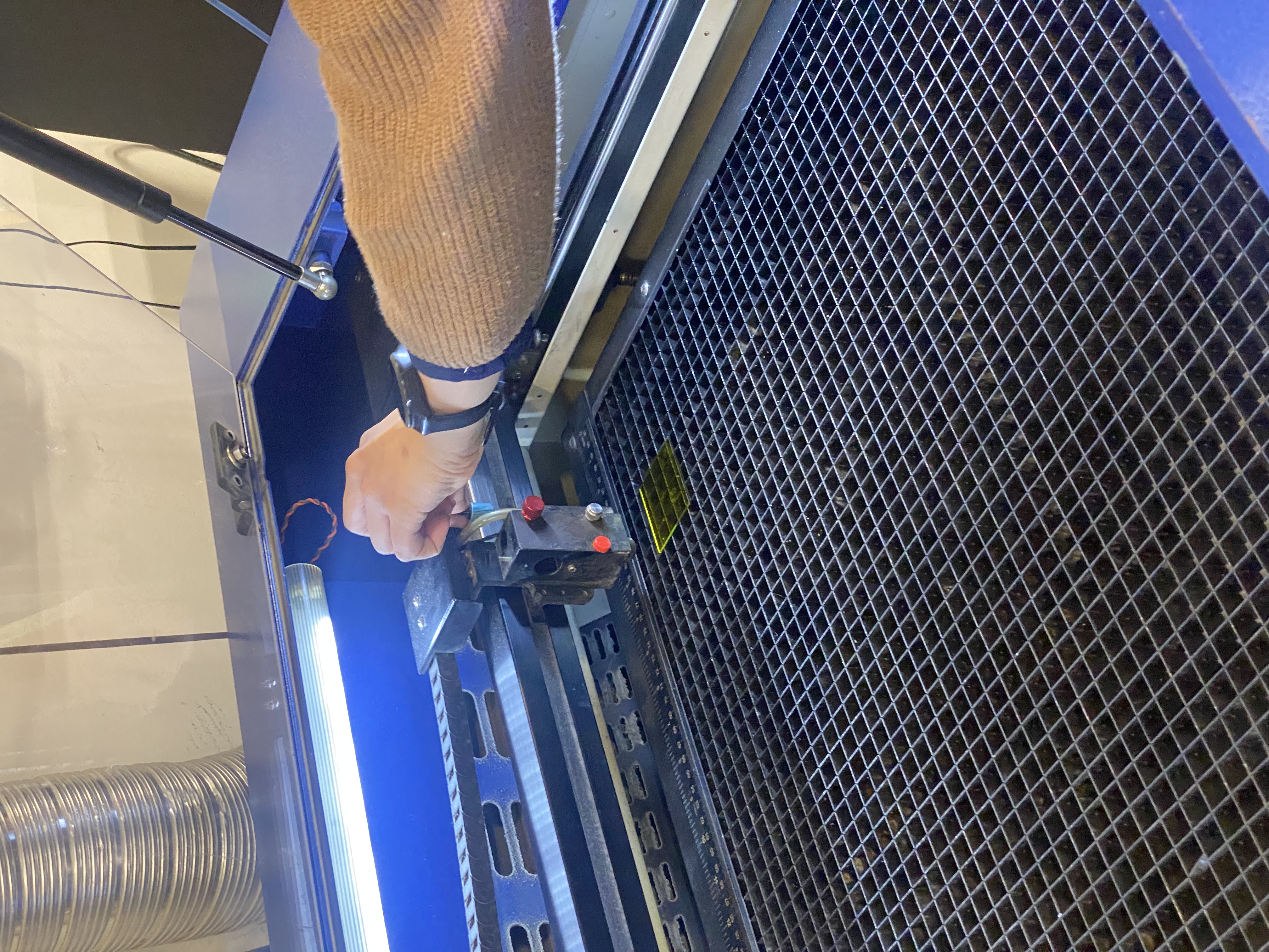
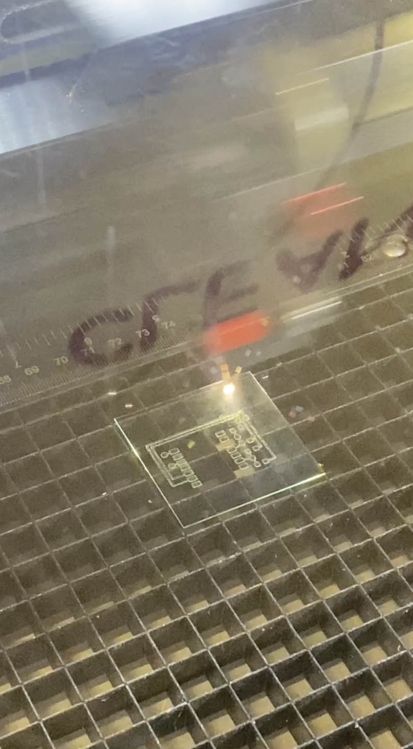
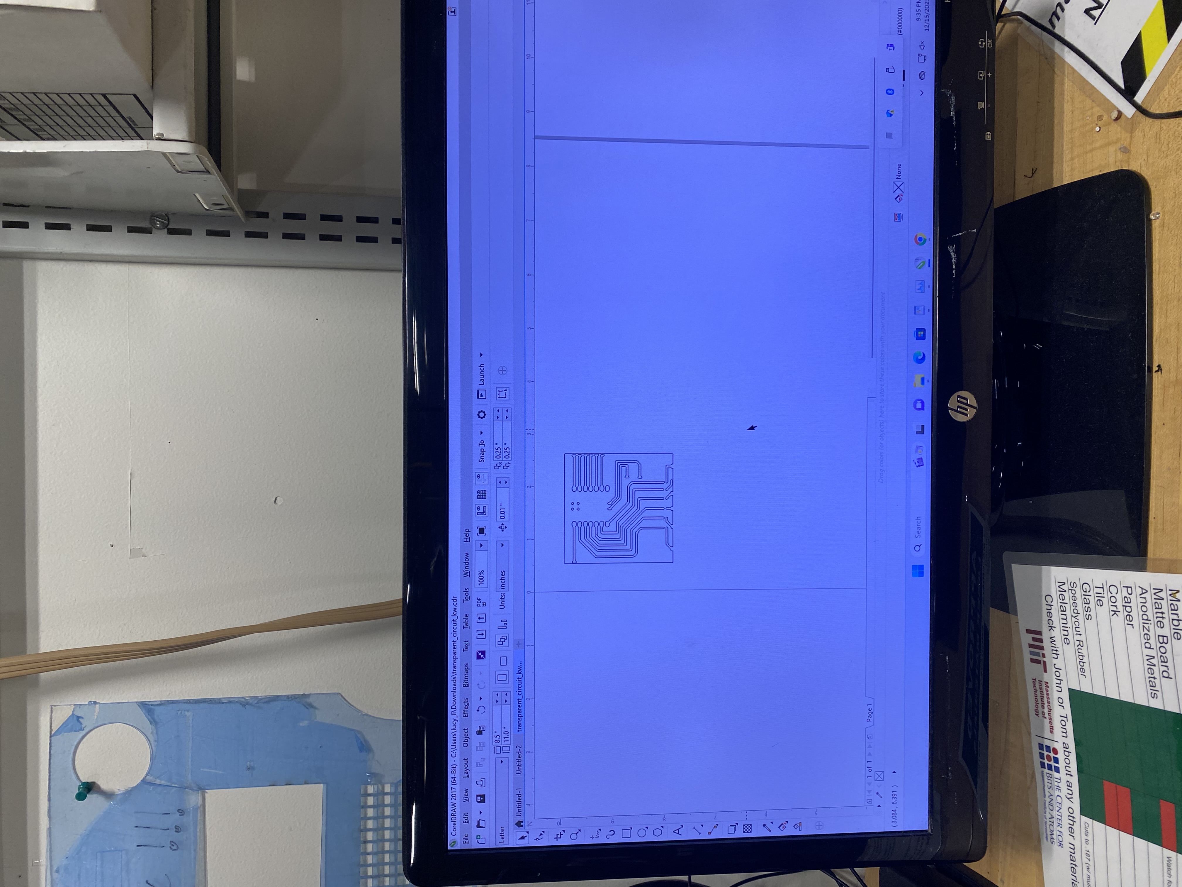
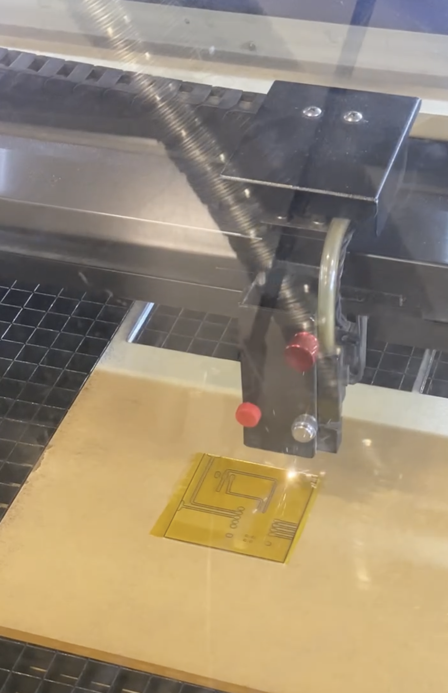
Import the SVG / DXF file
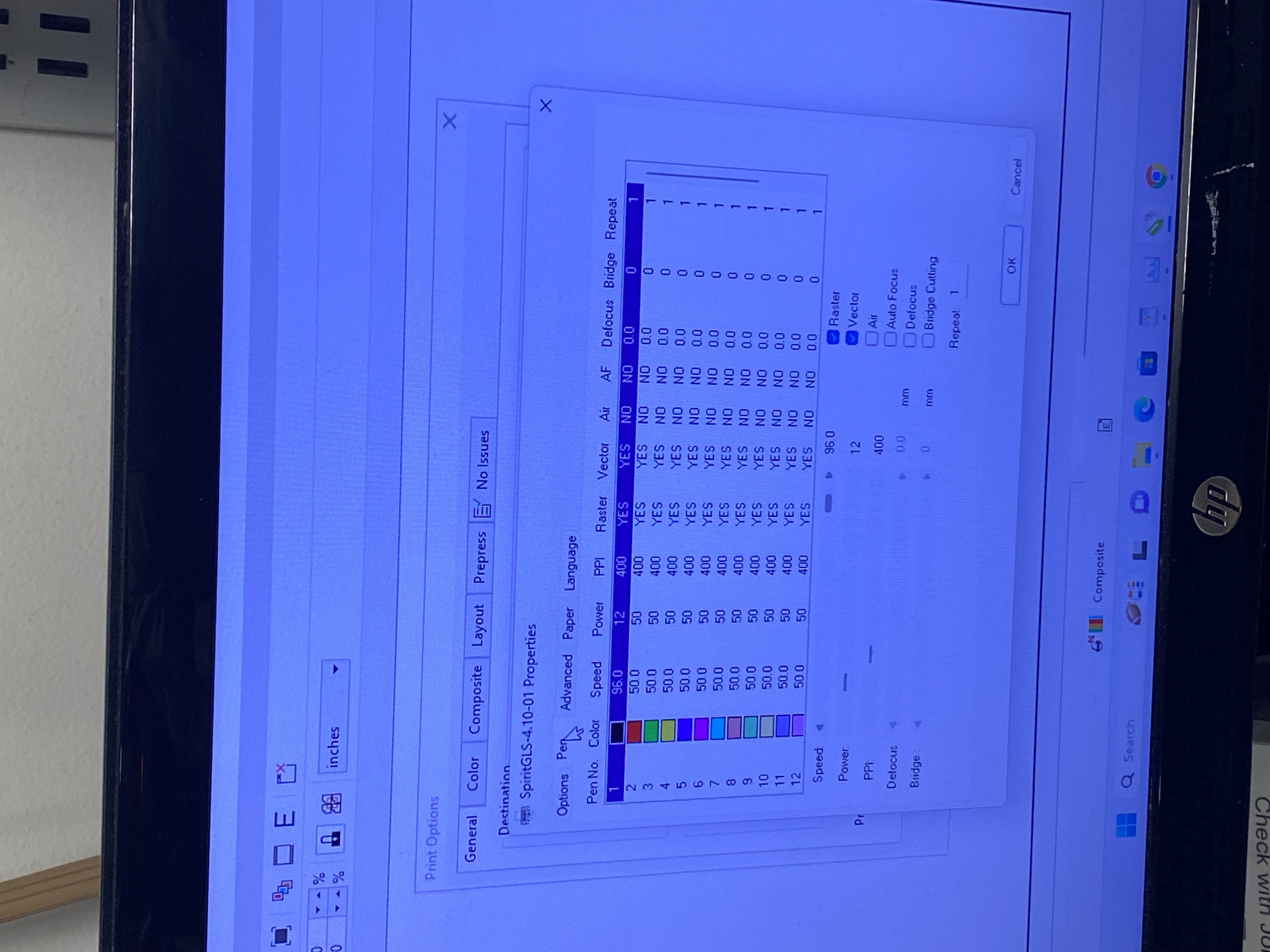
To know where the laser will operate, first raster the sacrificial layer to precisely know where it cuts

Make sure it leaves the mark to place the glass
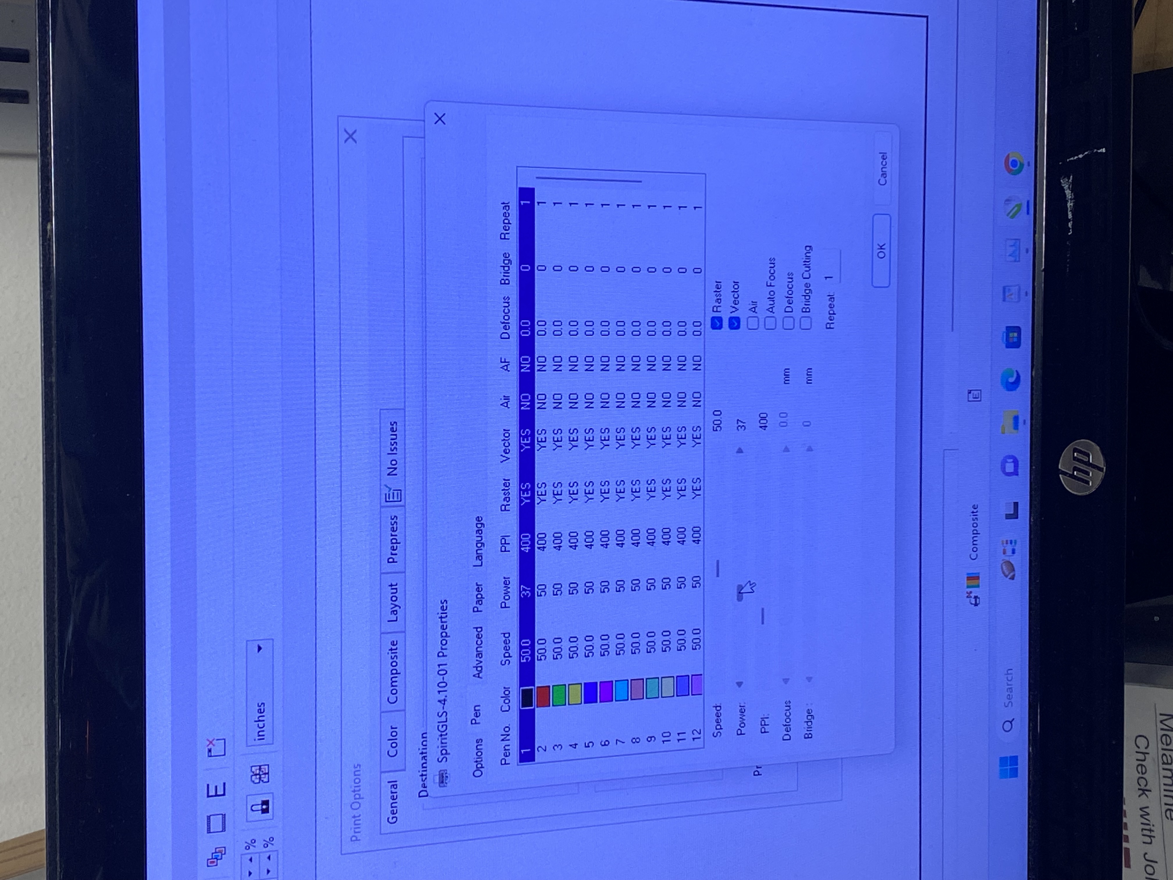
Now change the setting to do the actual cutting of the masking tape


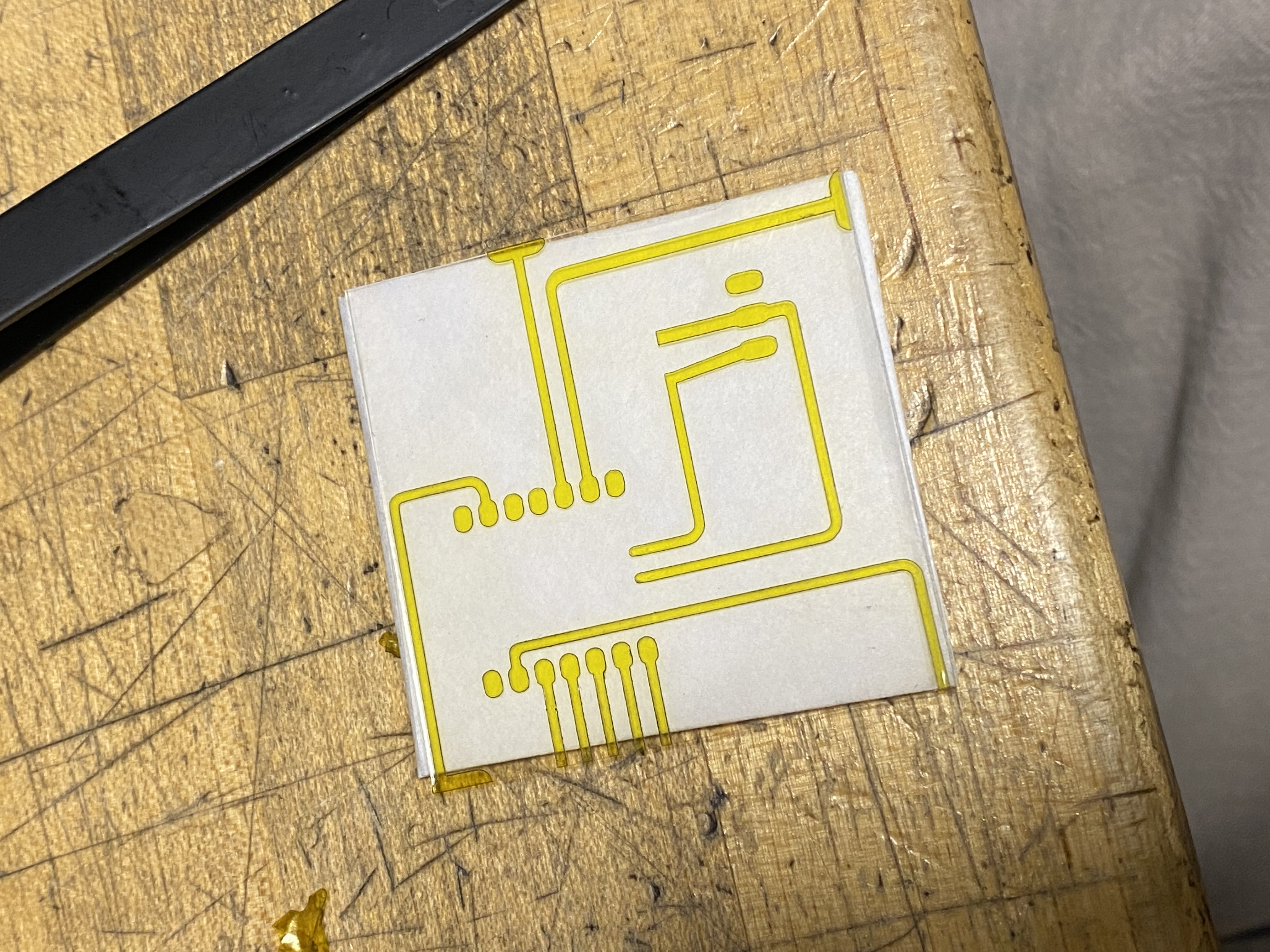
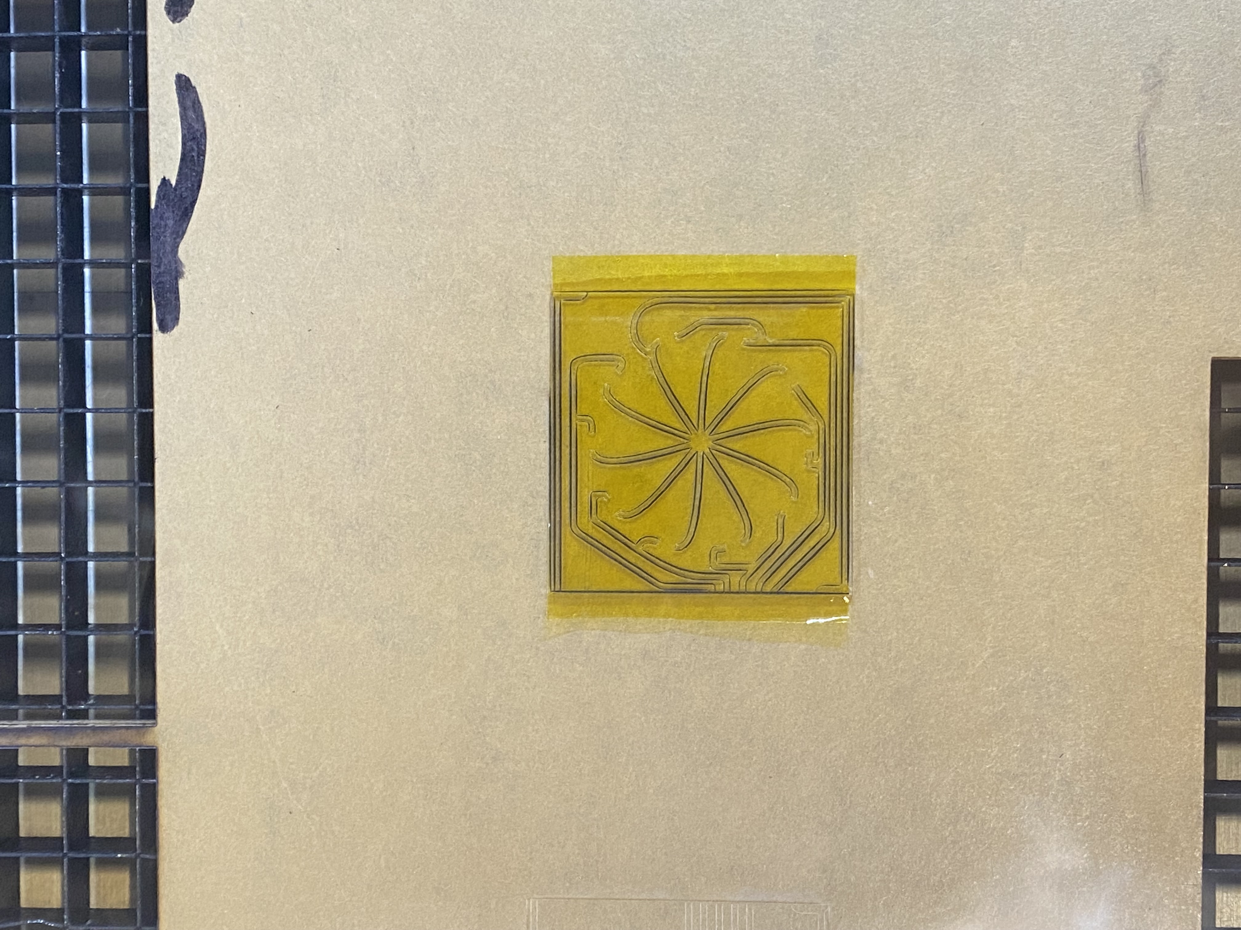
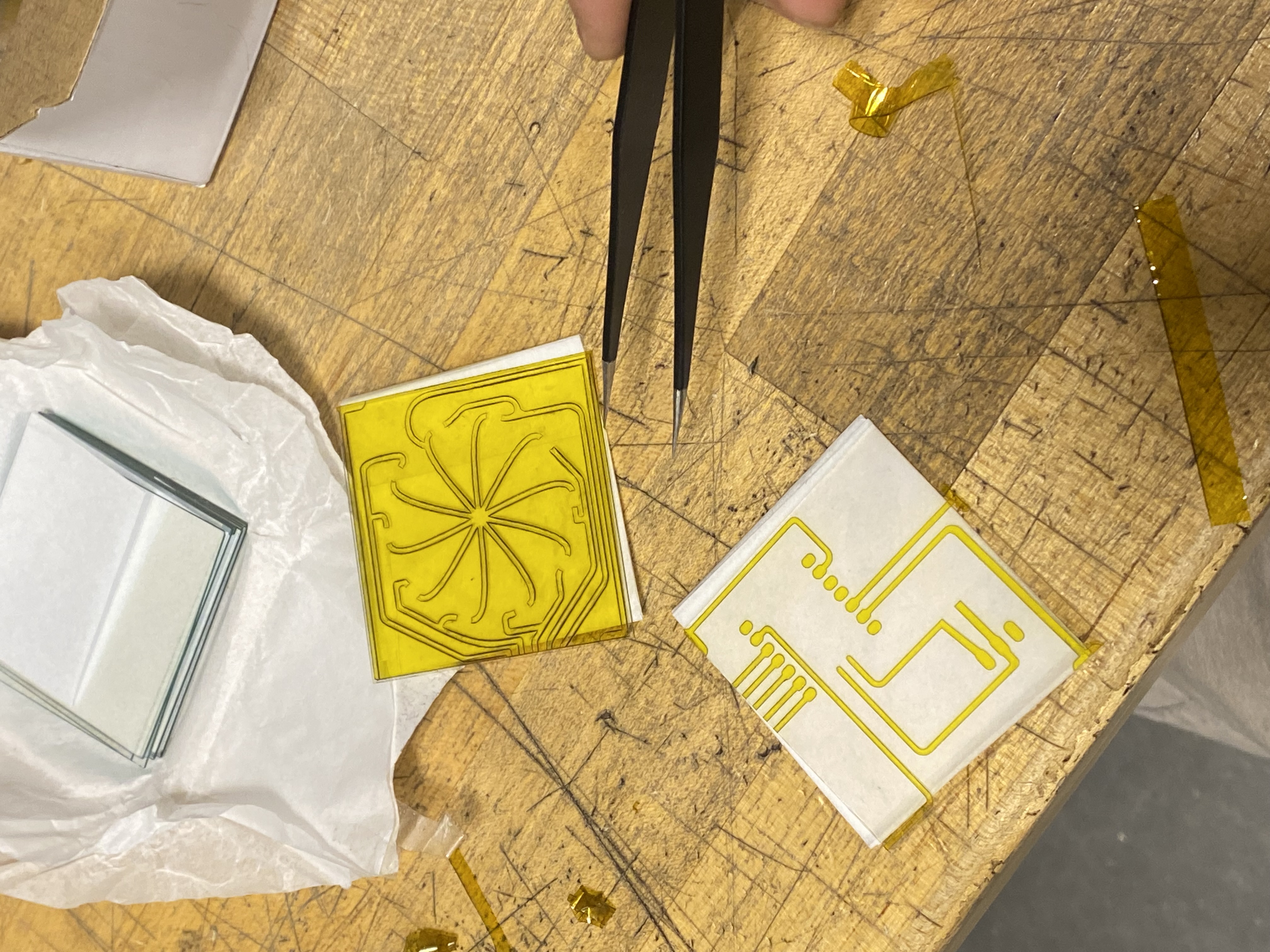
Taking off the part that doesn’t need conductivity
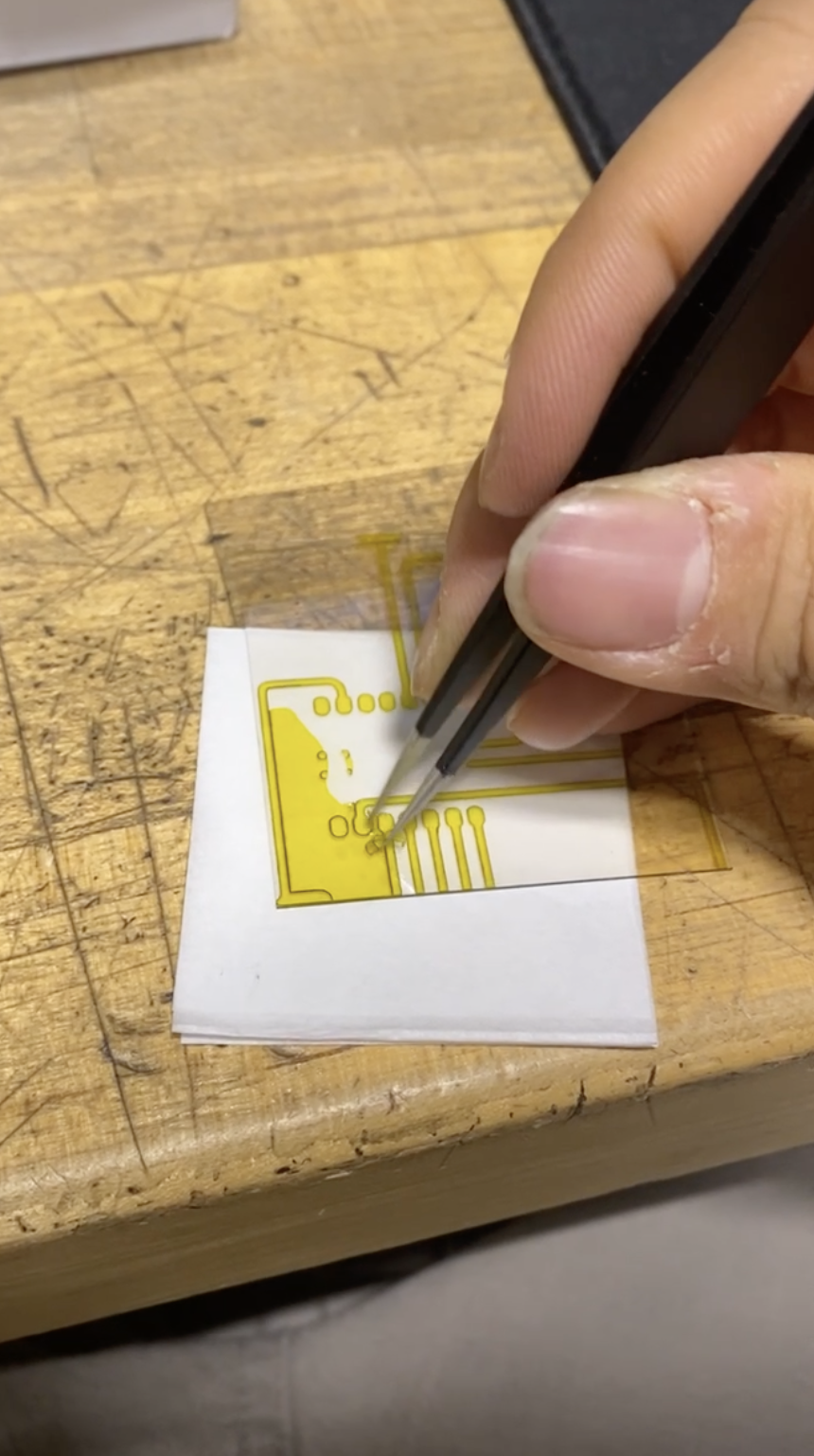
Using tweezer helps
 Sometimes Laser doesn’t work properly even though the settings are same
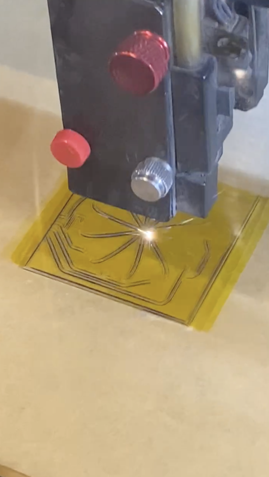
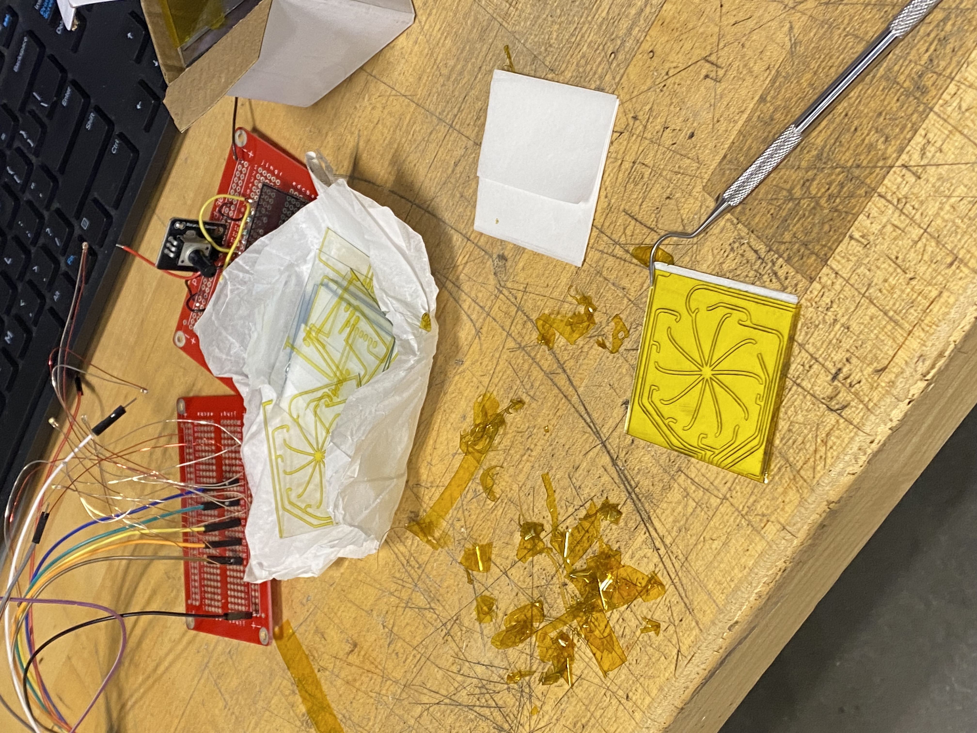
Re-cutting
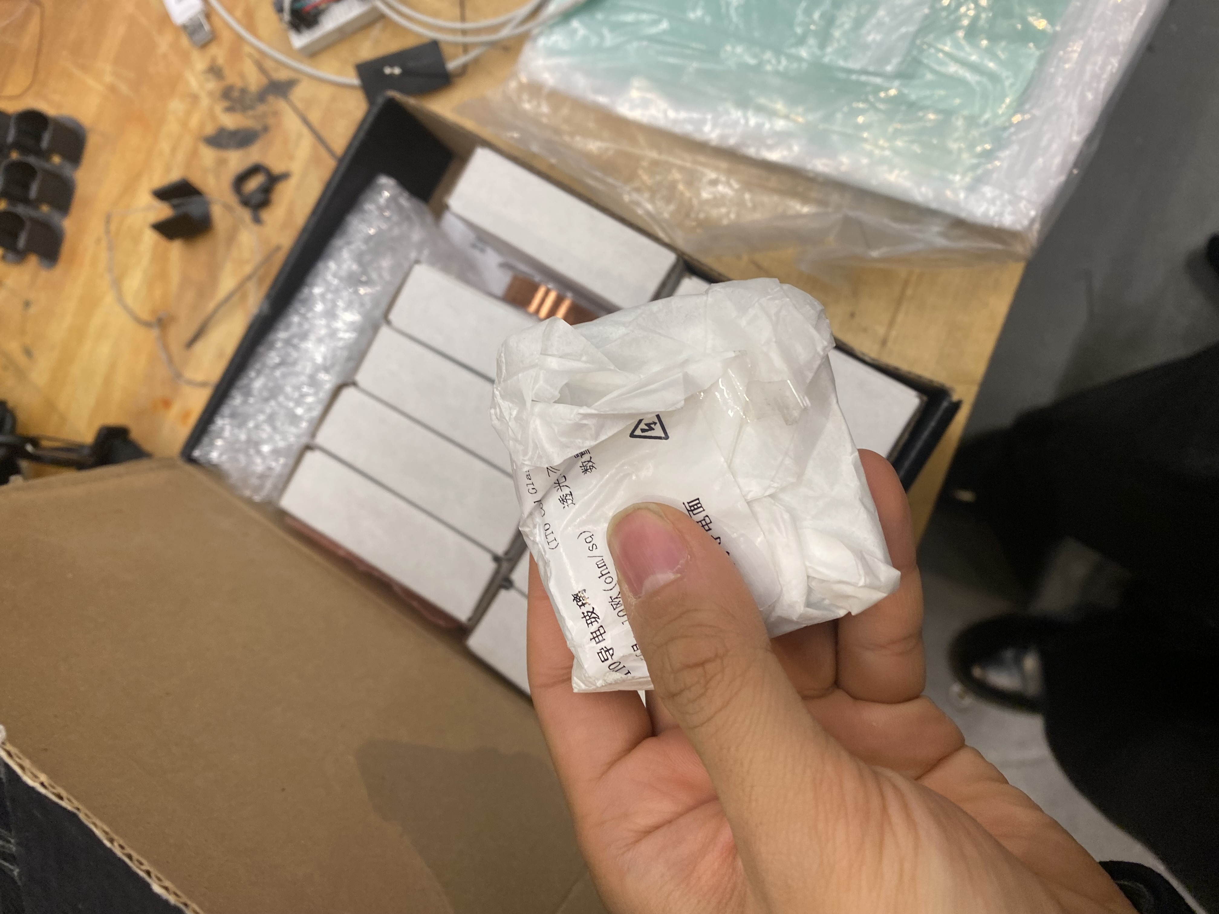
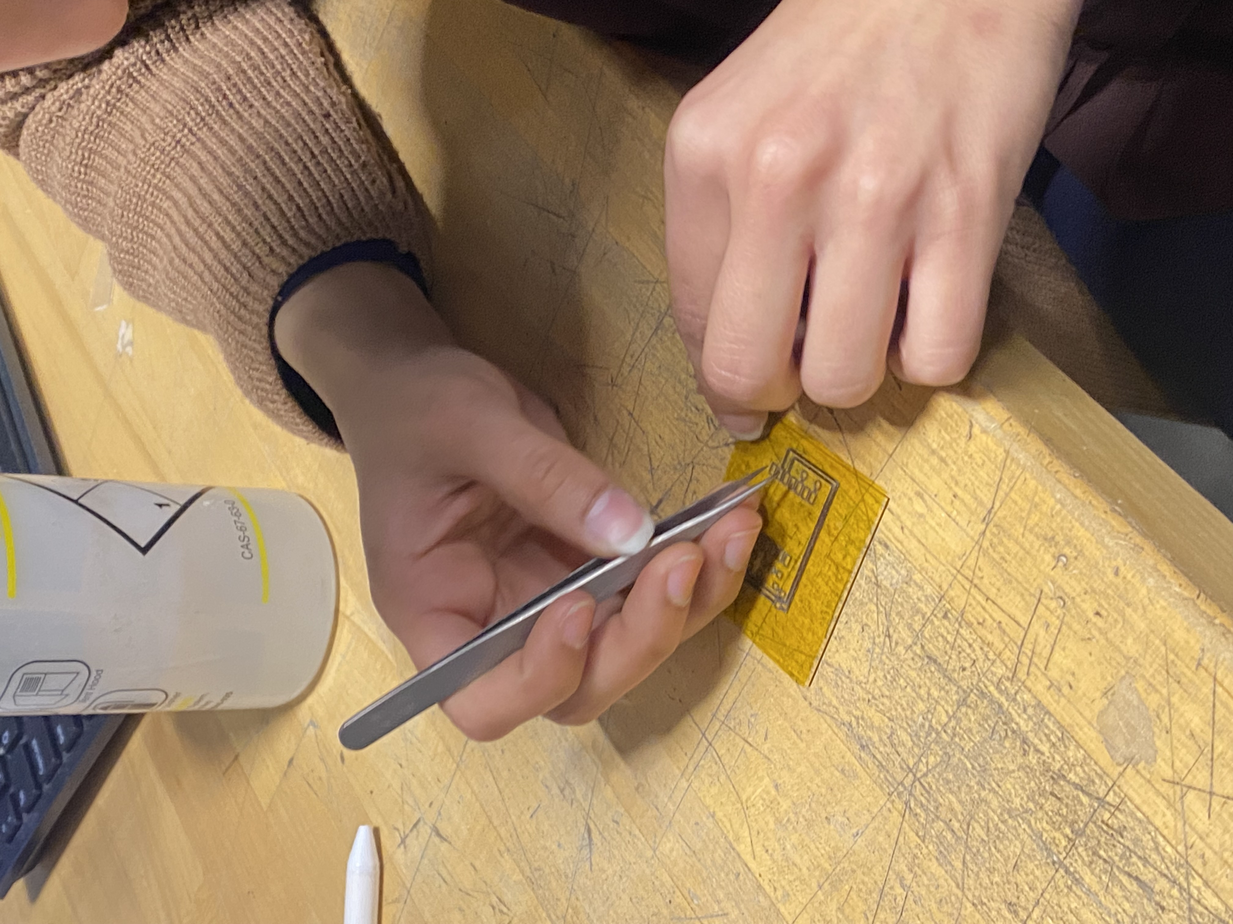
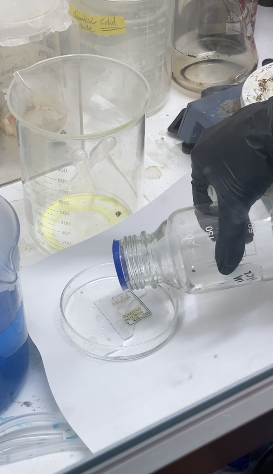
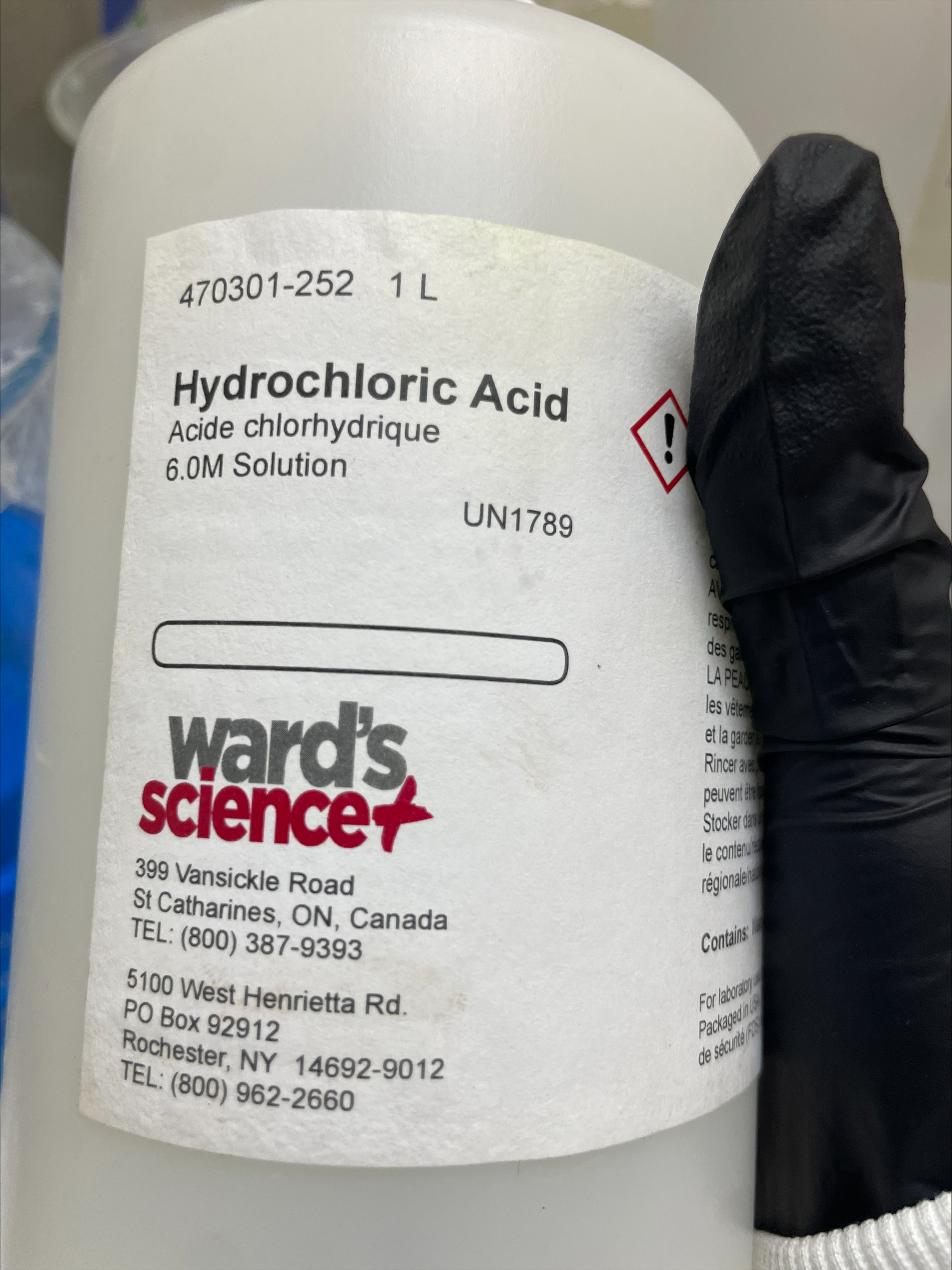
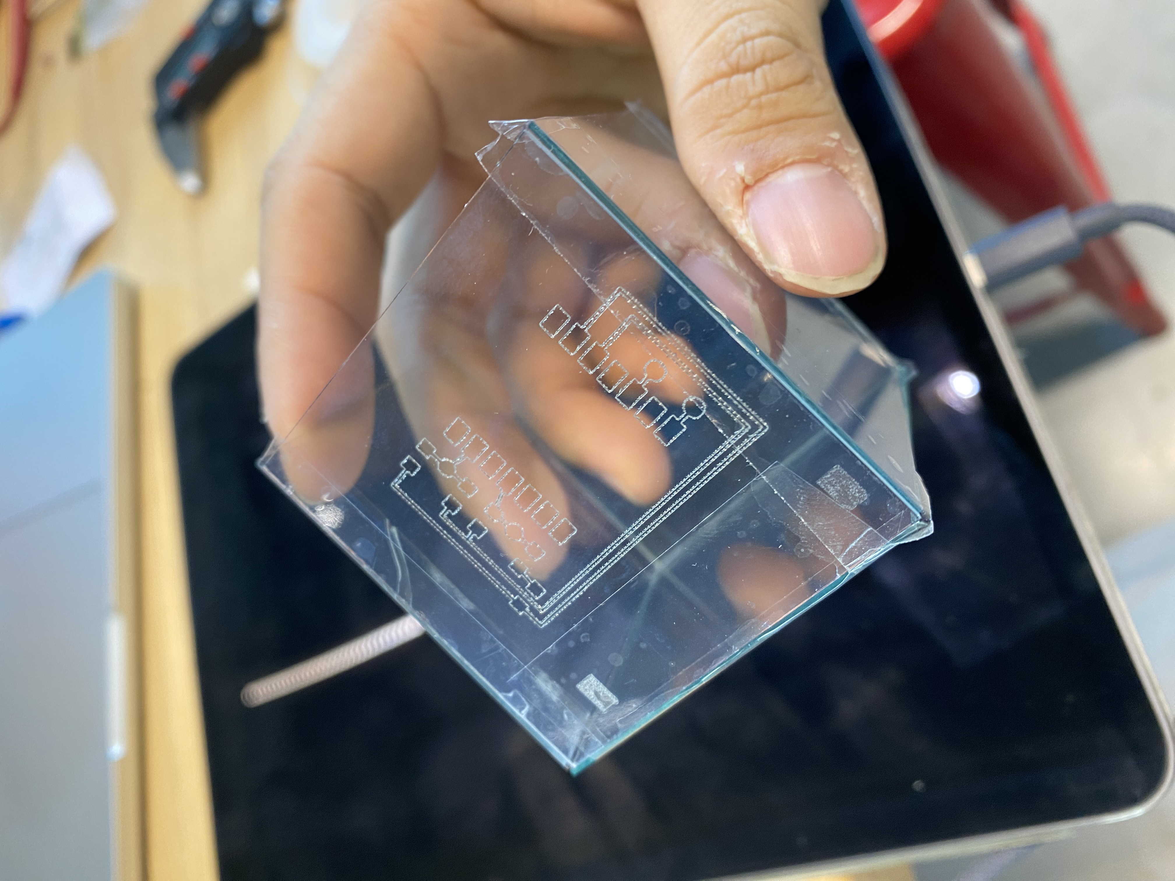
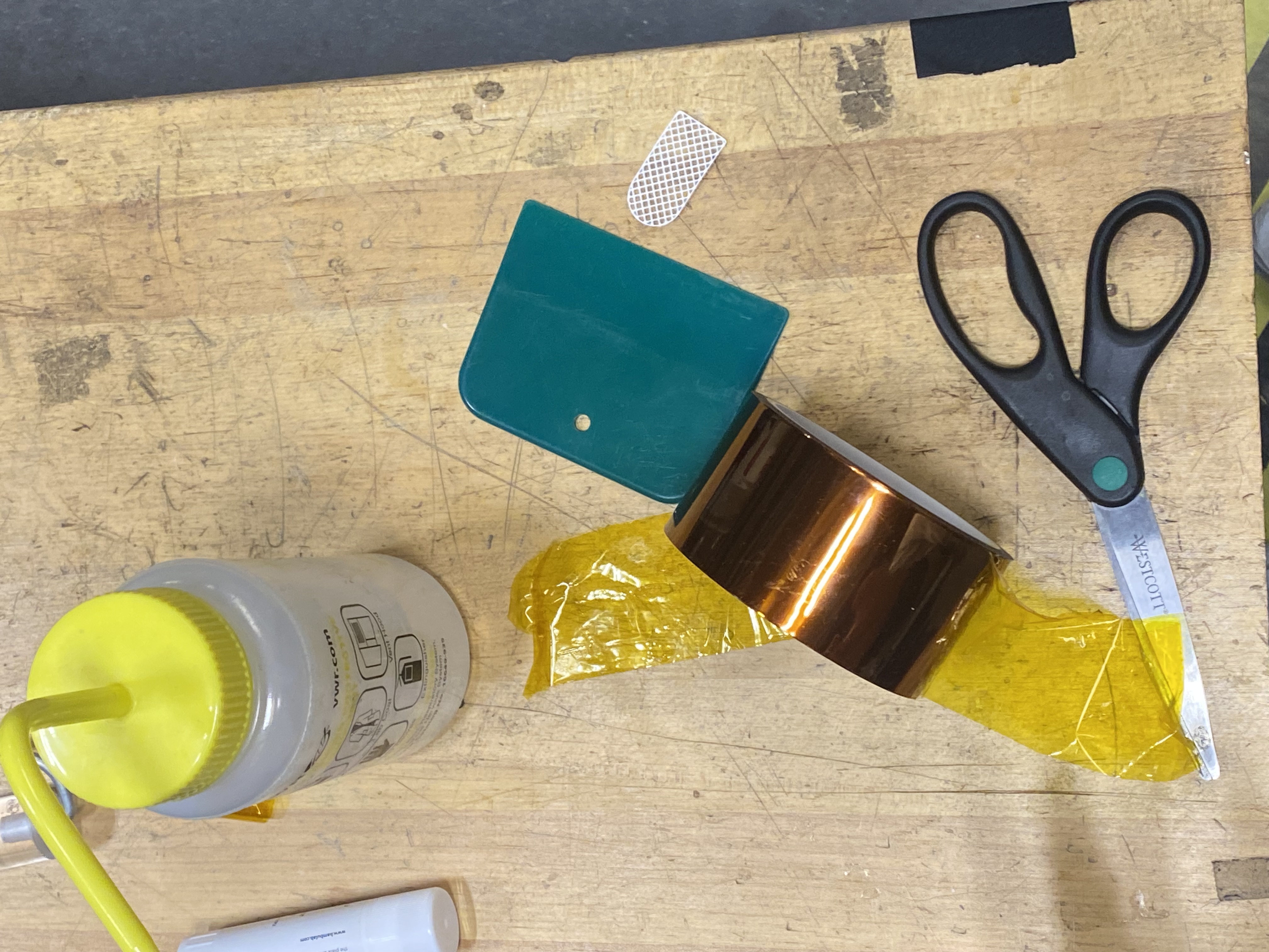
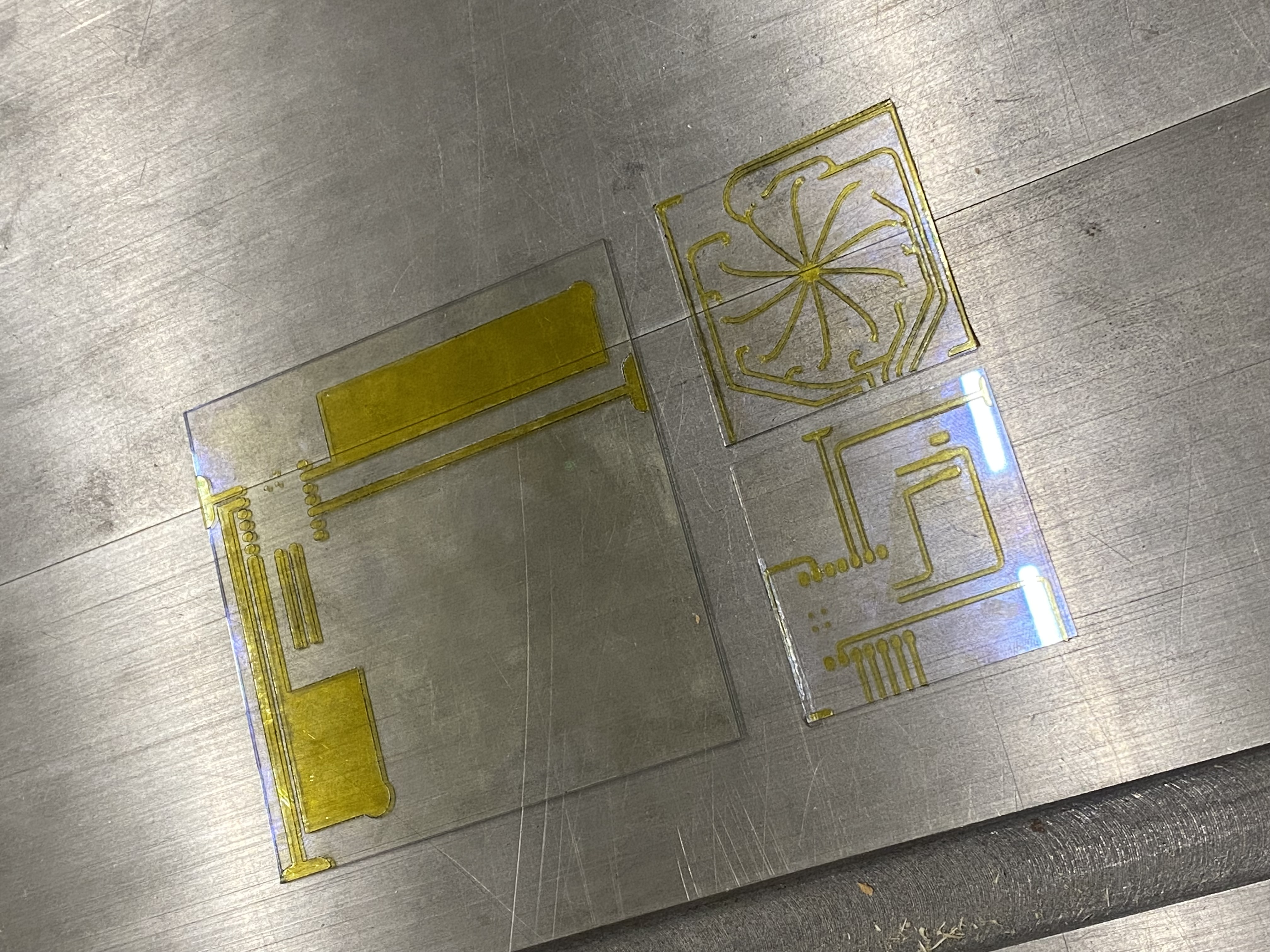
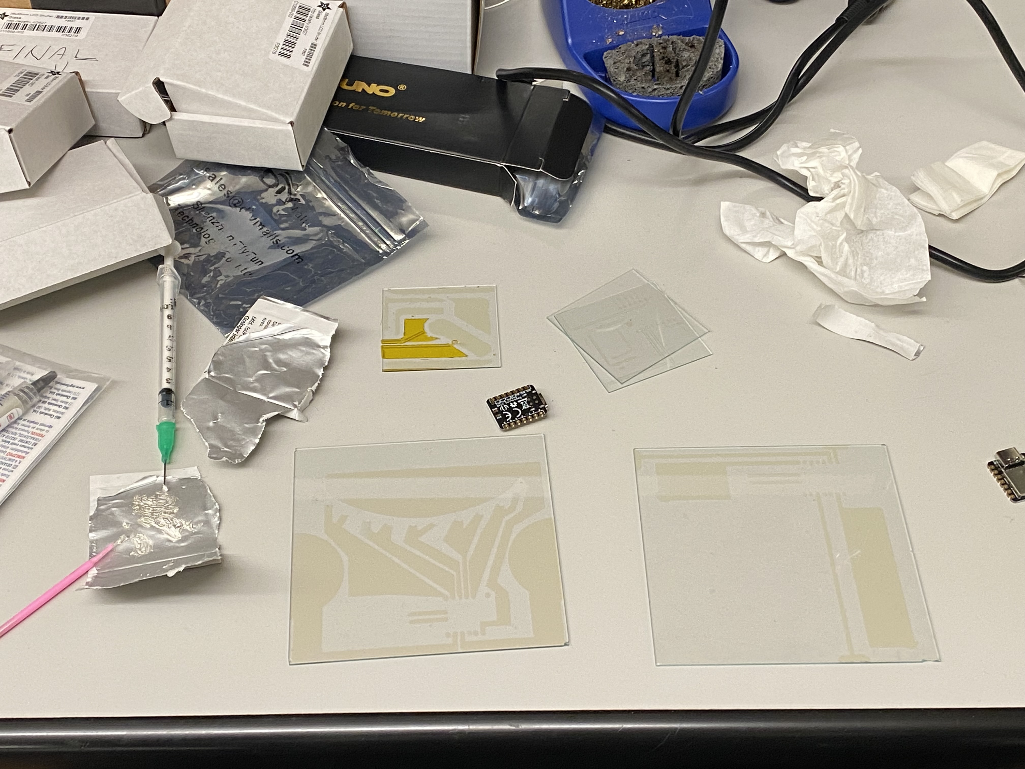
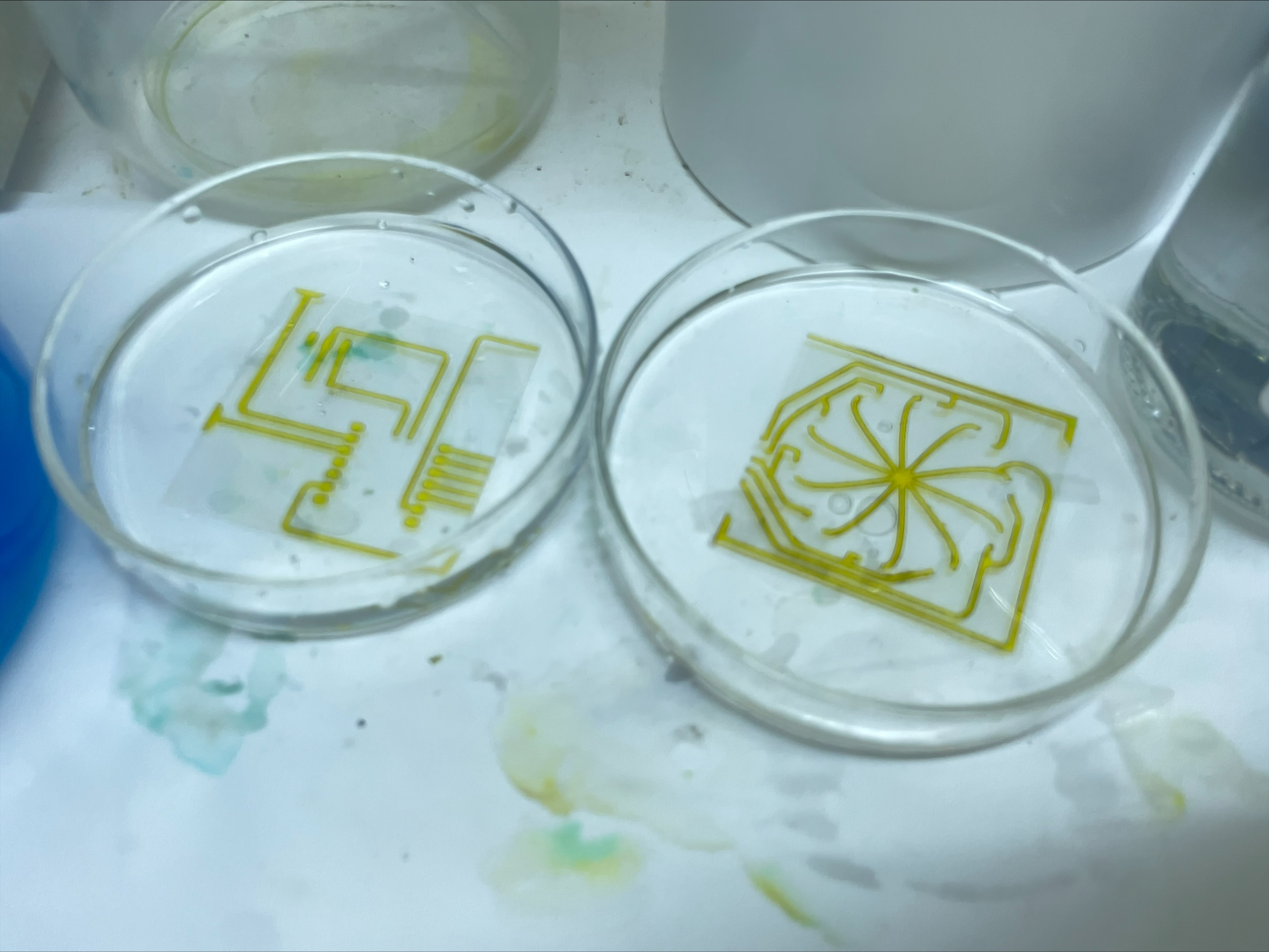 Putting the samples into Hydro chloric Acid Solution
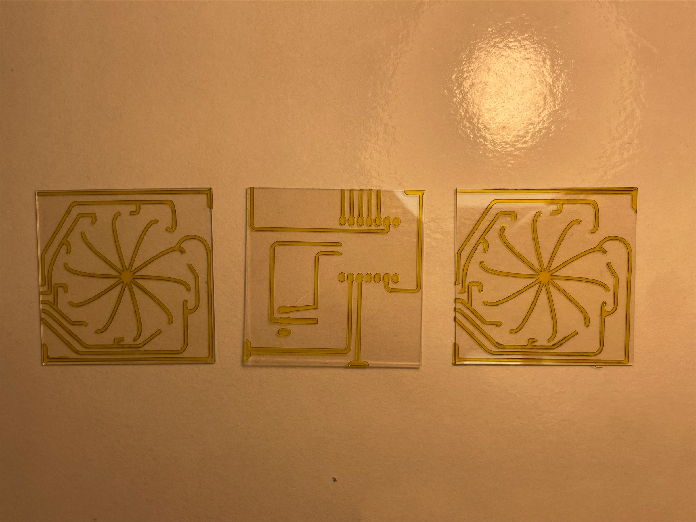
The first experiment were done with 1 Molar of hydrochloric acid (meaning 1 mol/Liter of water)
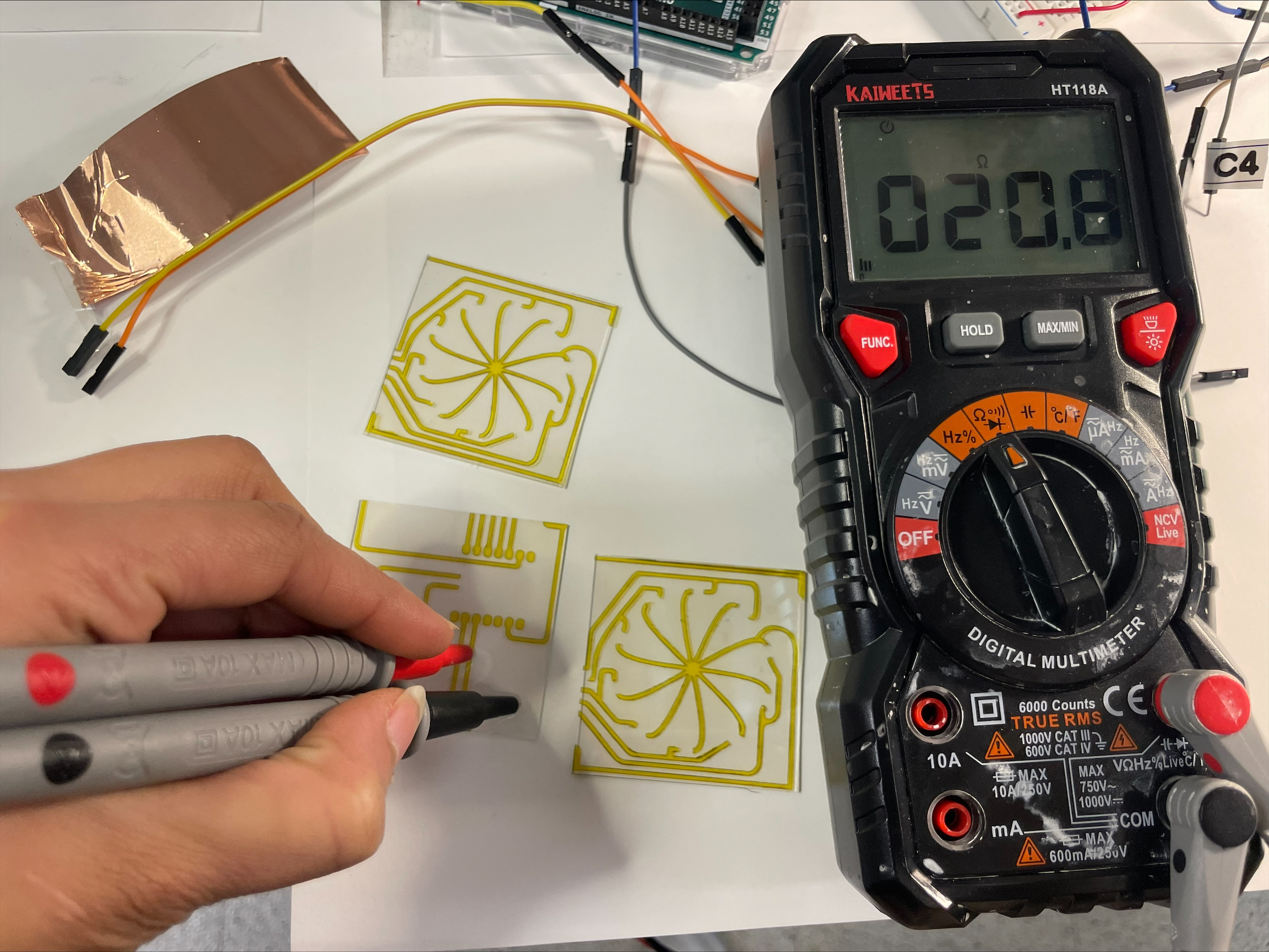
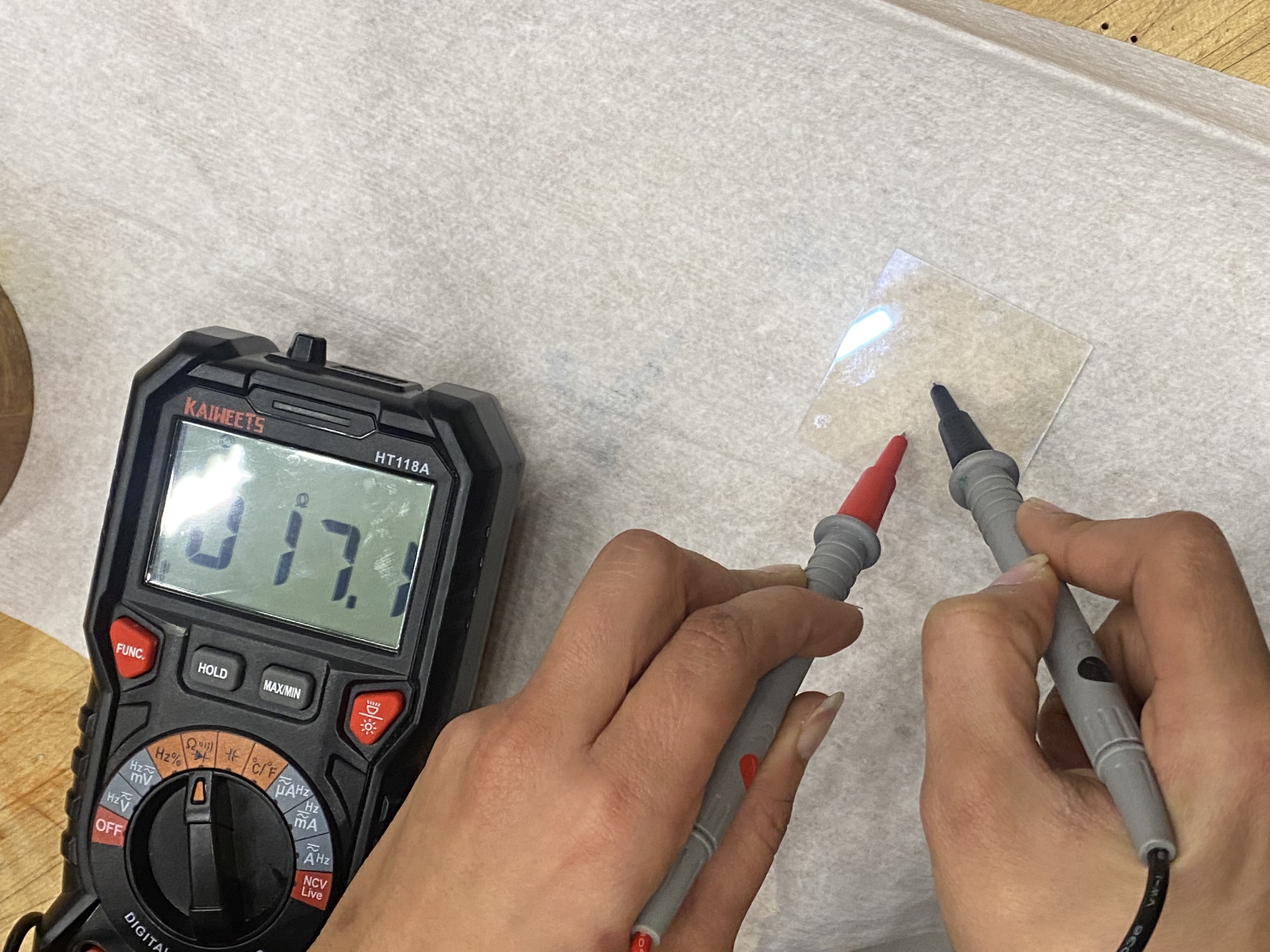
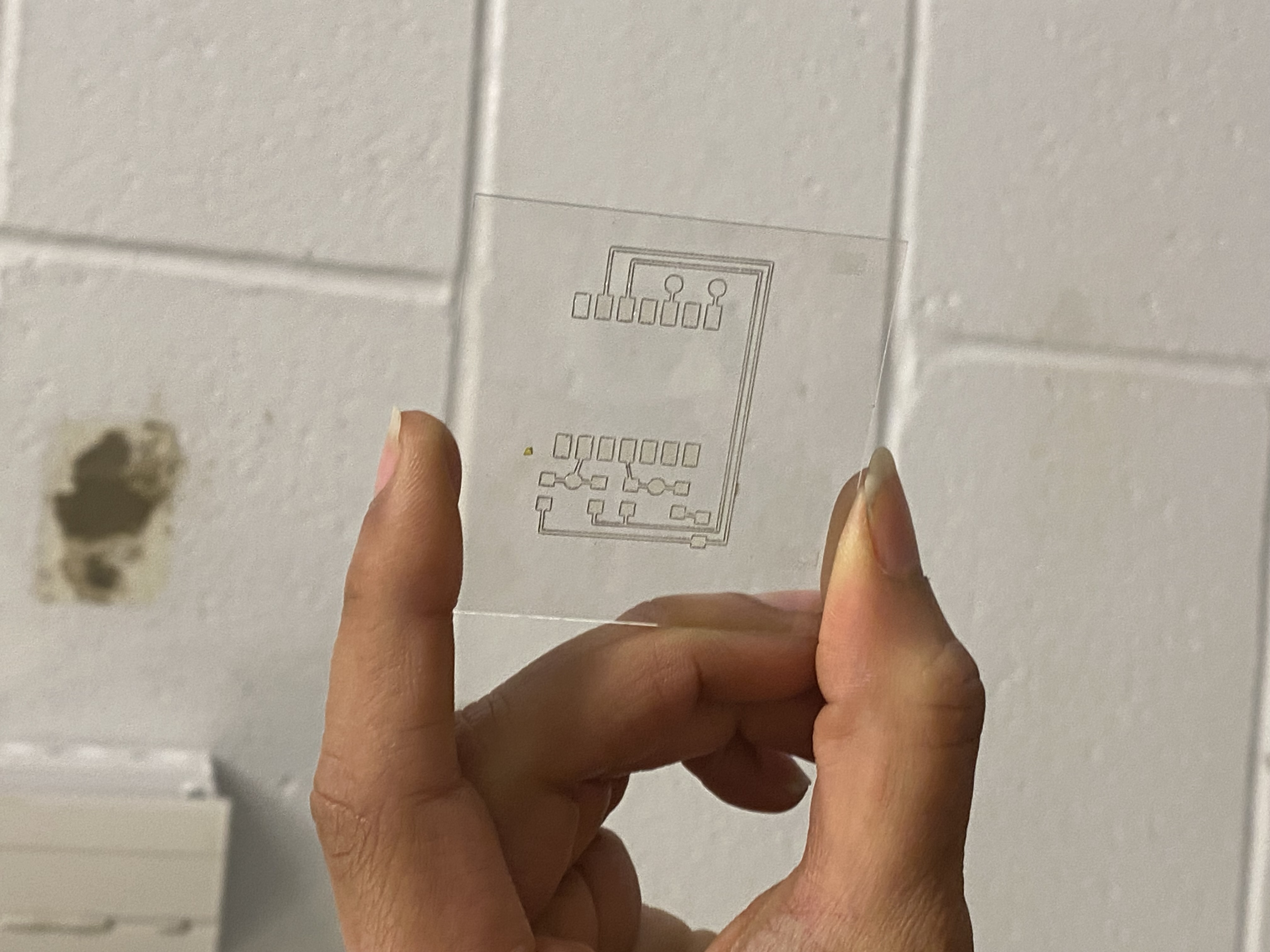
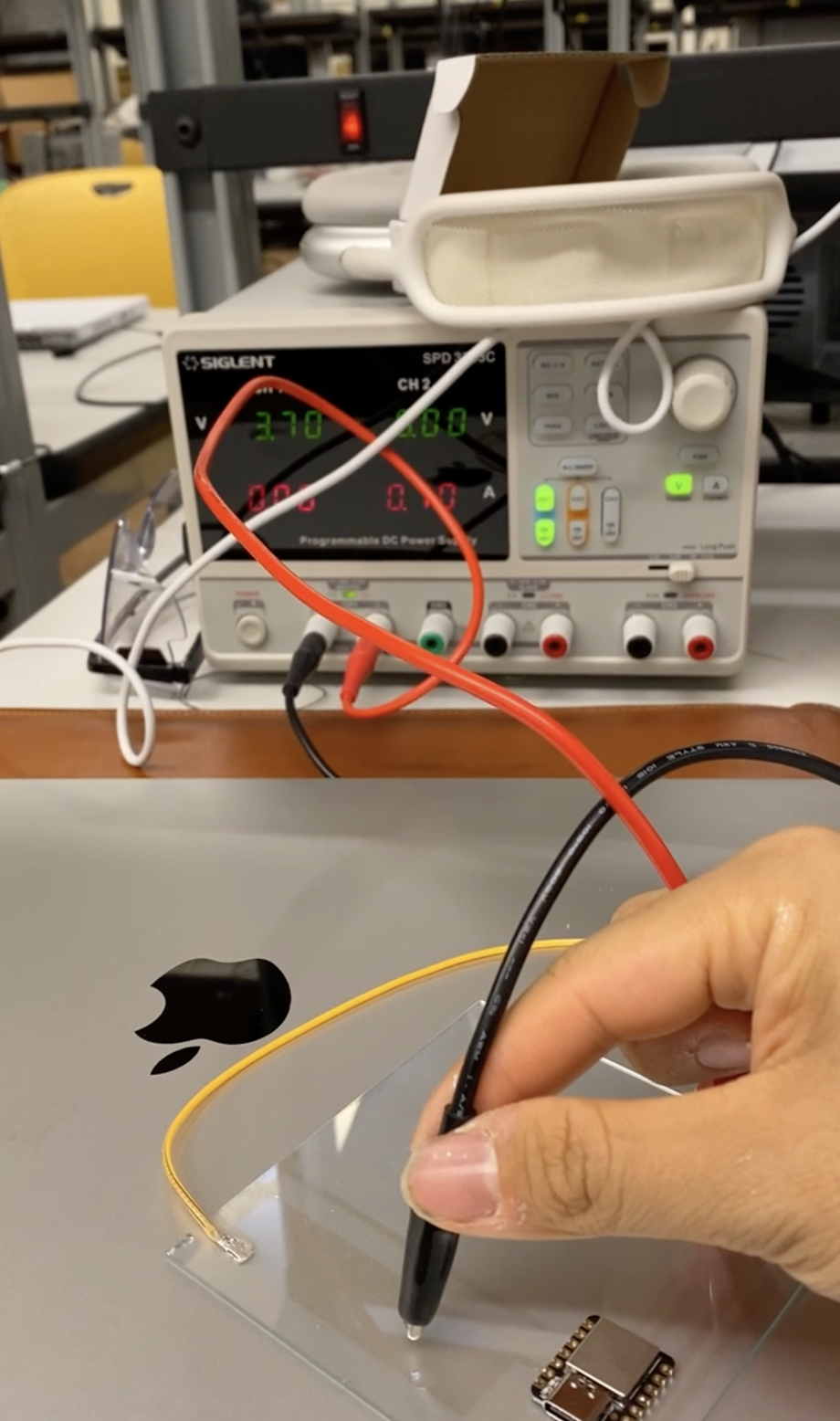
Checking the conductivity
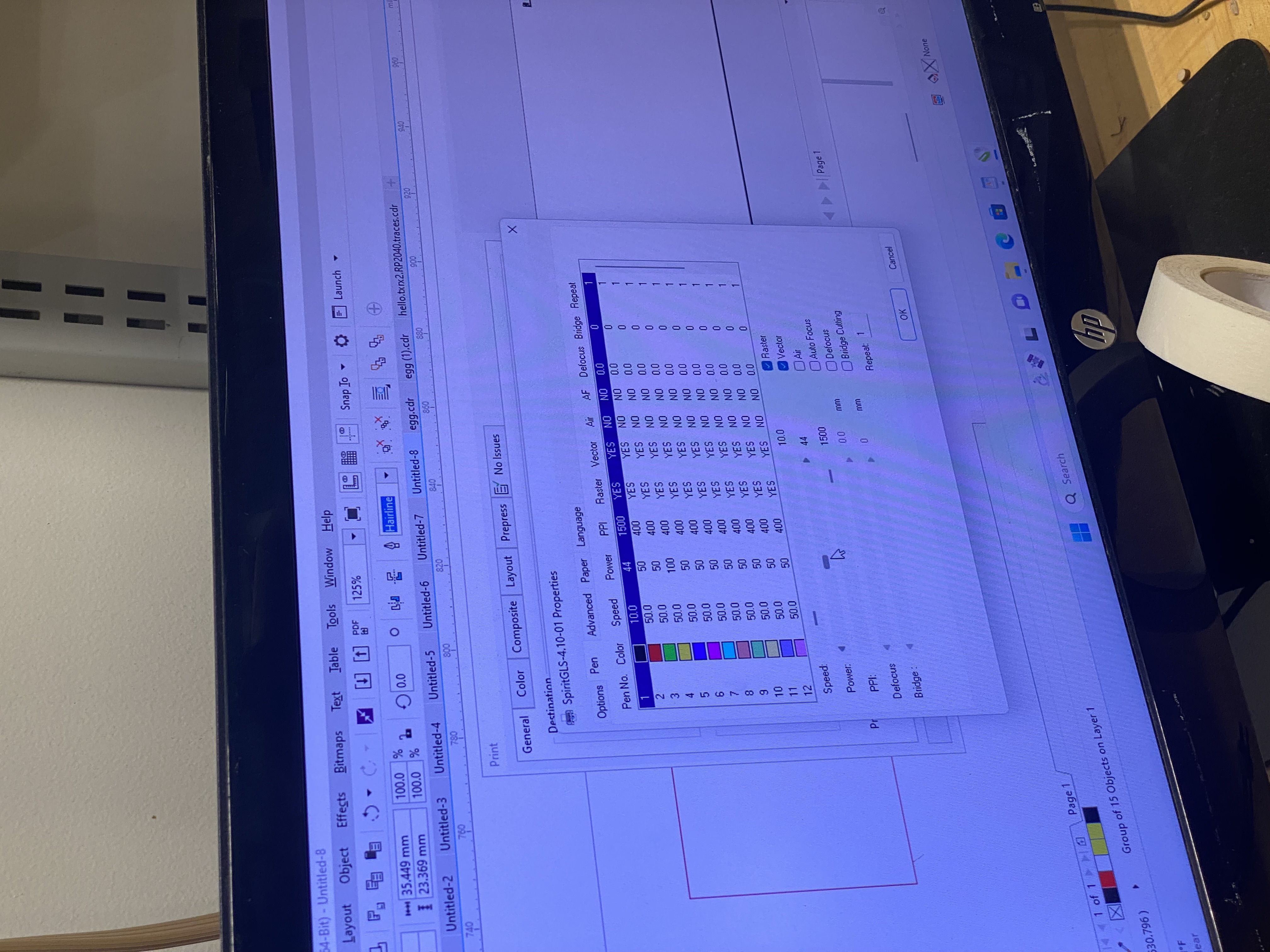
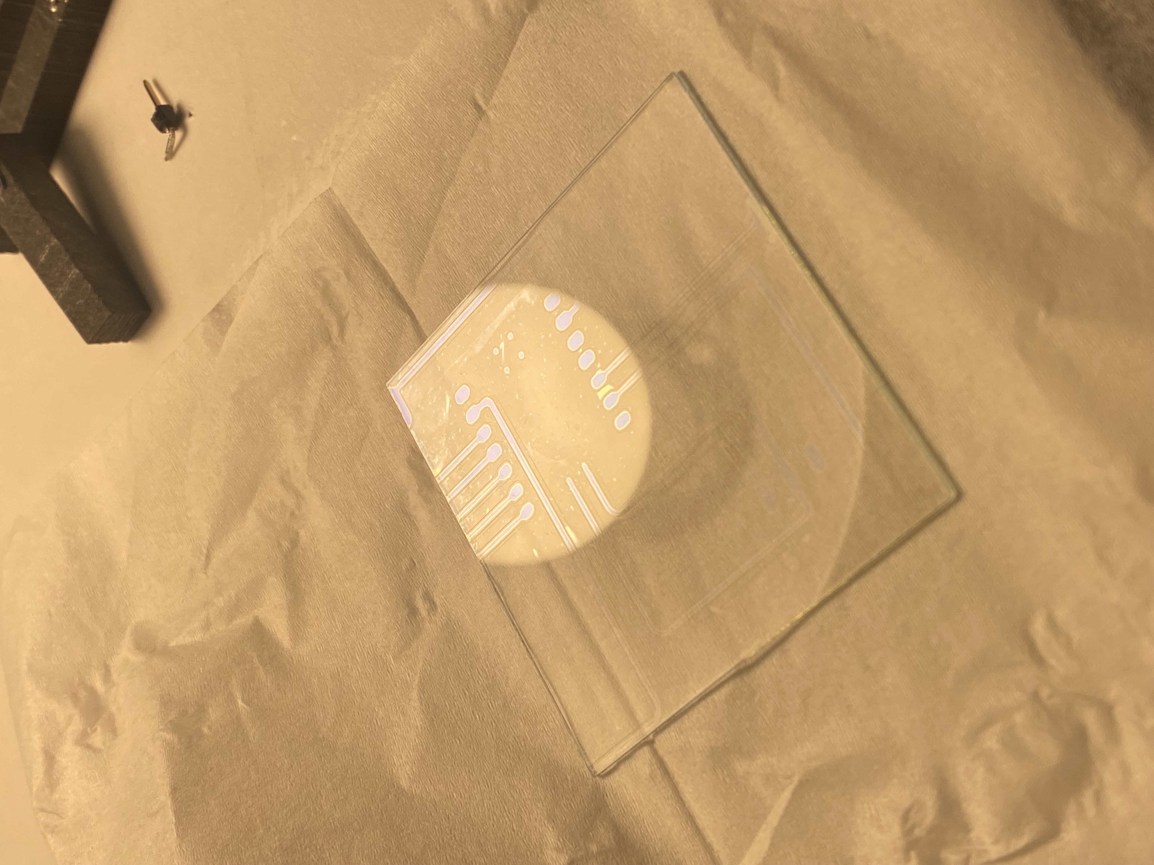 Output
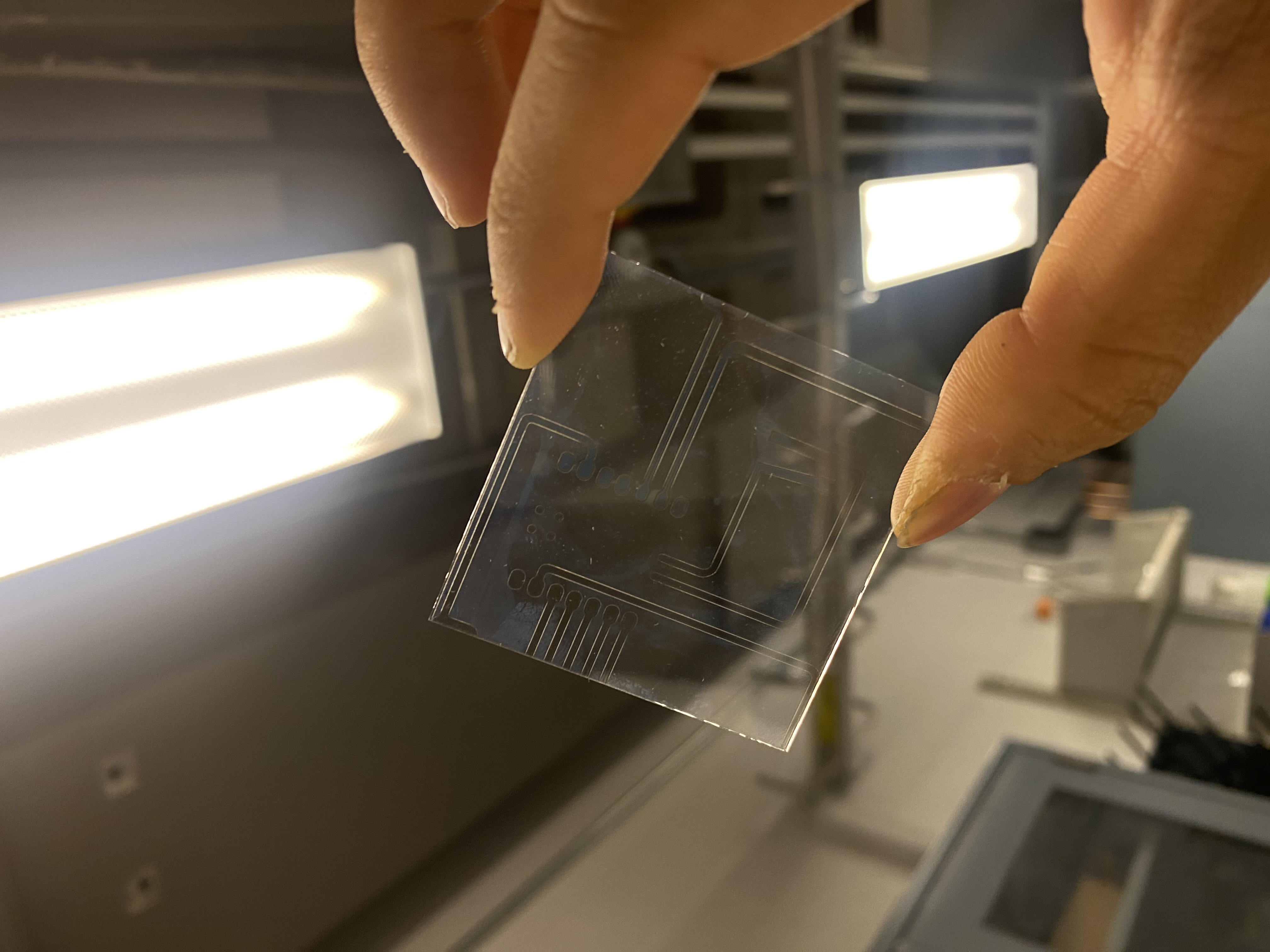

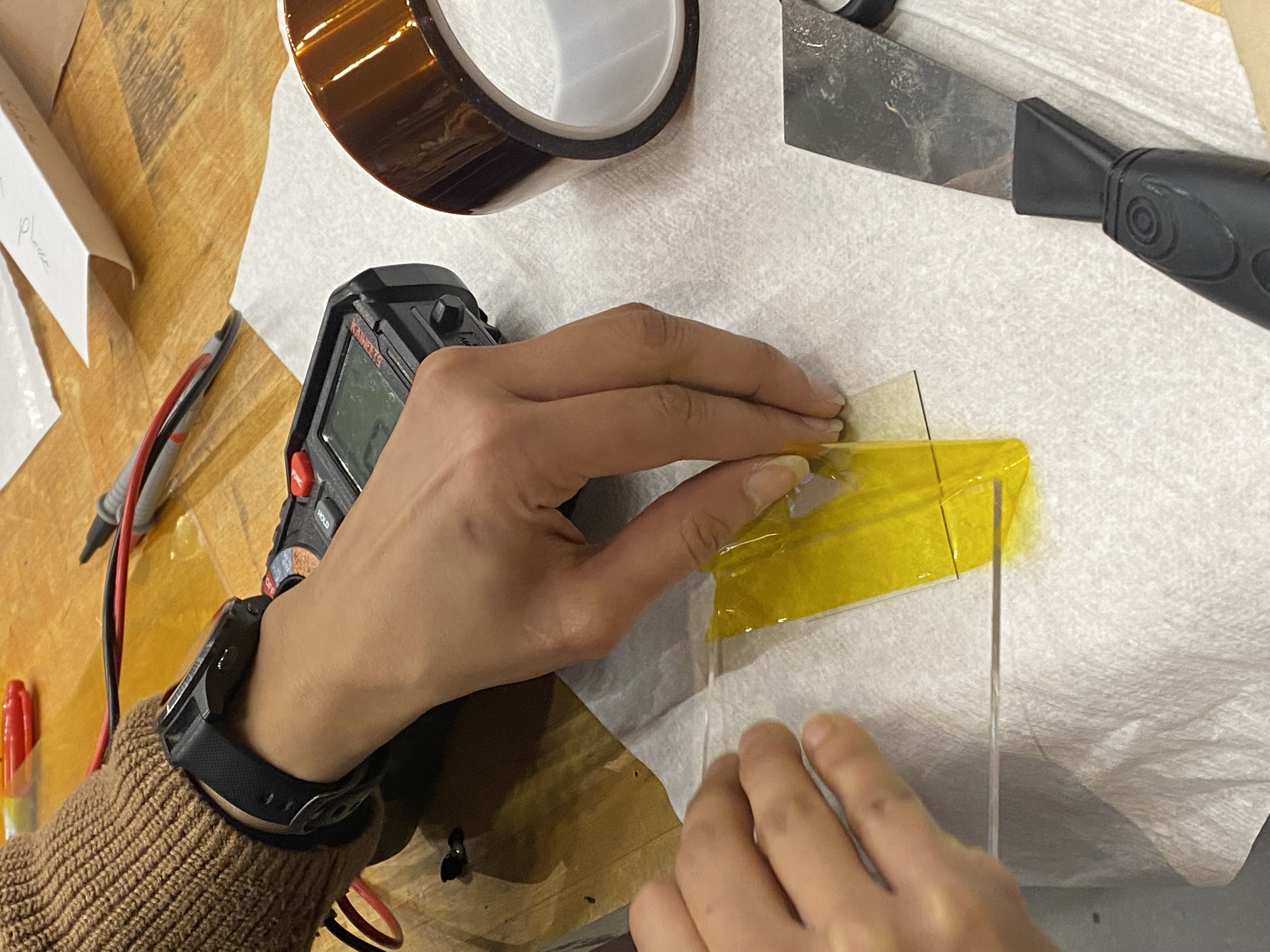
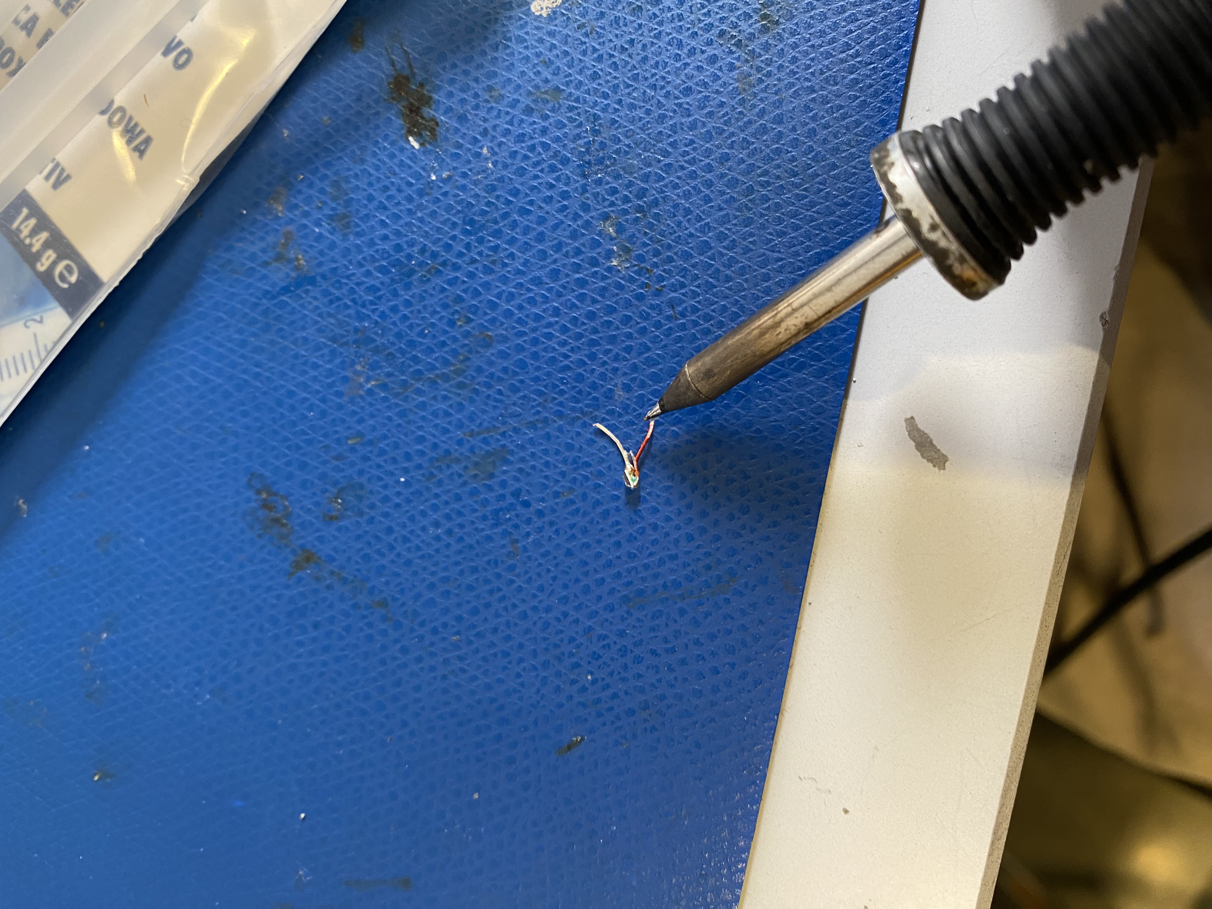
Preparing LEDs
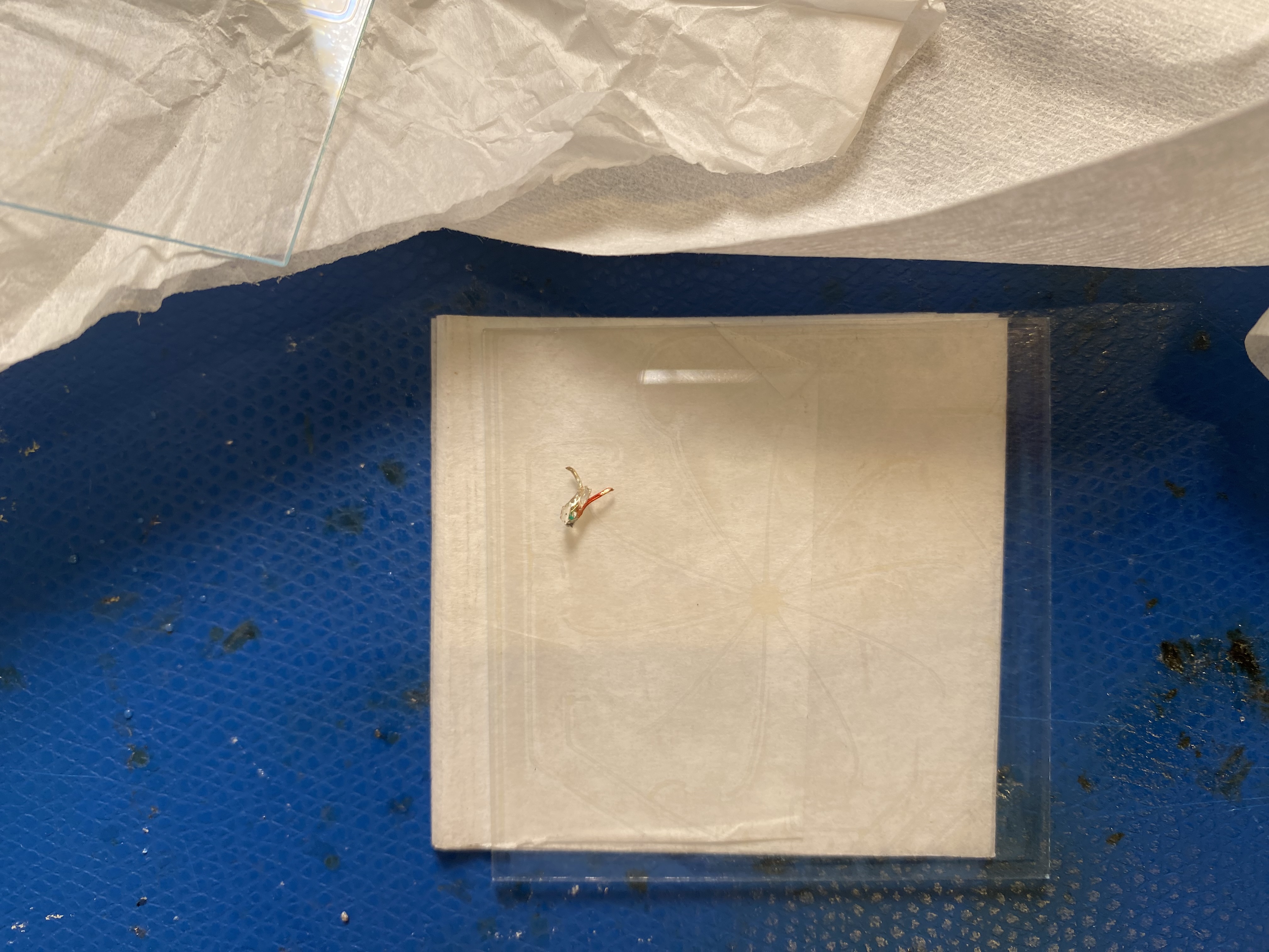
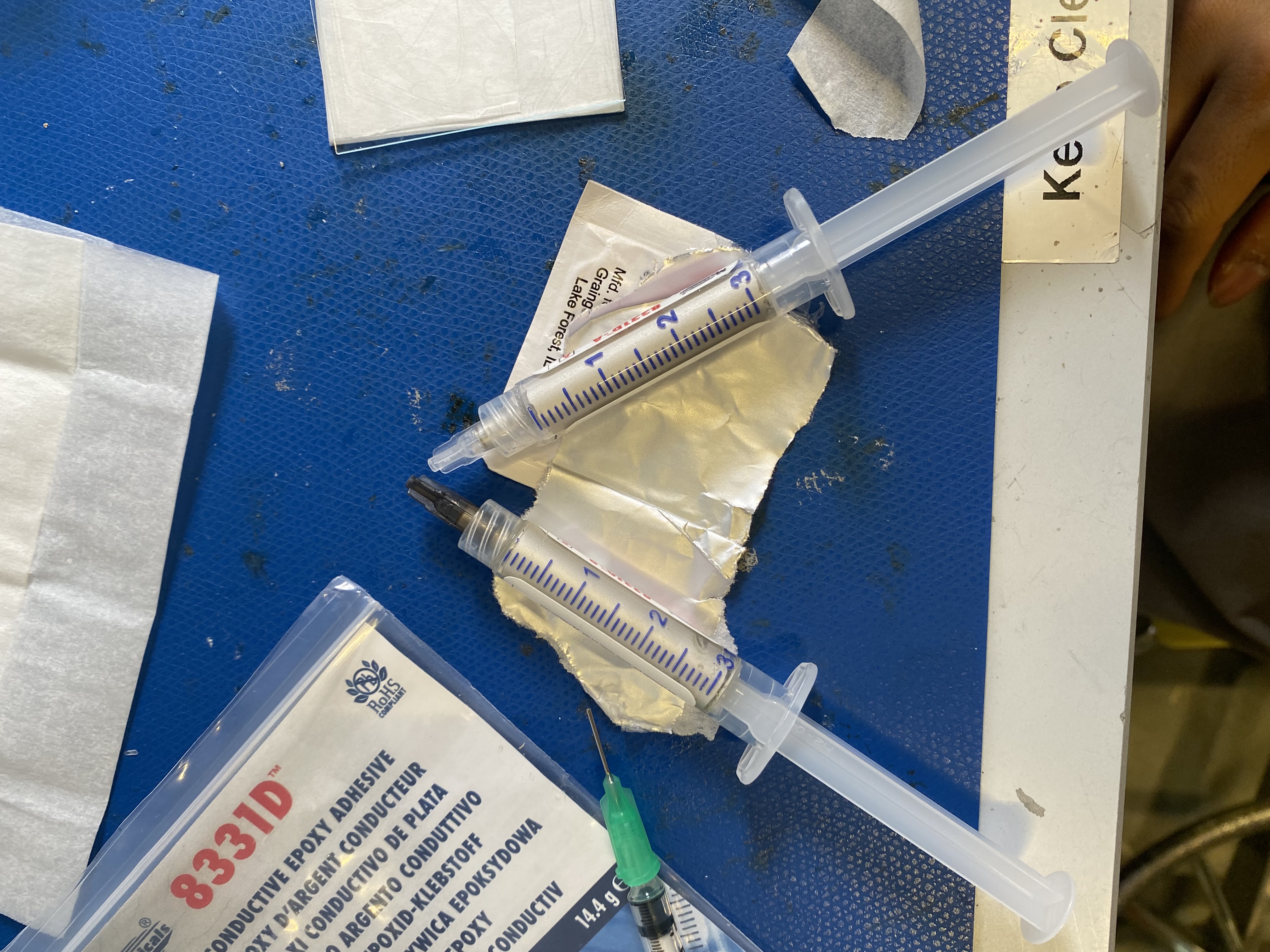
Preparing Silver Epoxy - As Glass doesn’t work with solder, I had to buy these ($100) to put components on the glass.
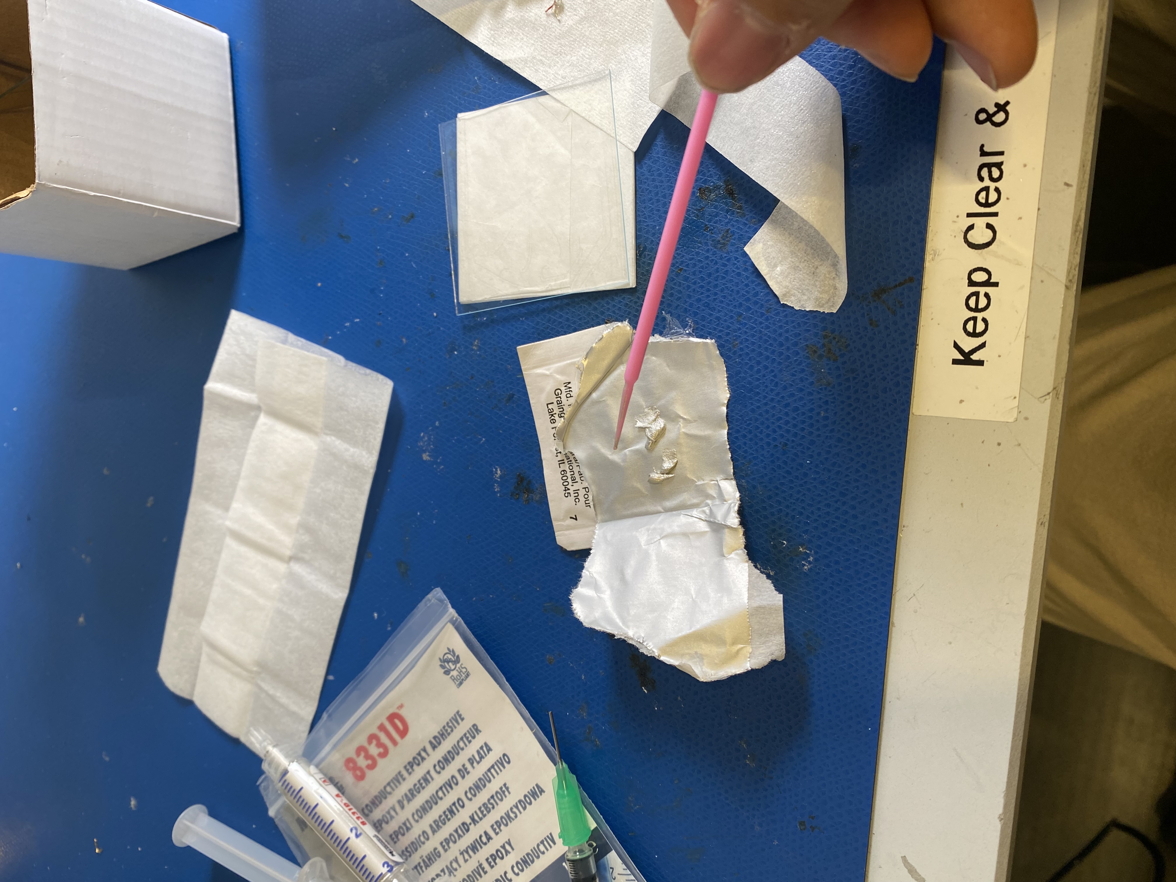
Mixing the A,B parts of the epoxy
Using applicator for delicate control

It turned out that with only a very little amount,
They can be bridged easily
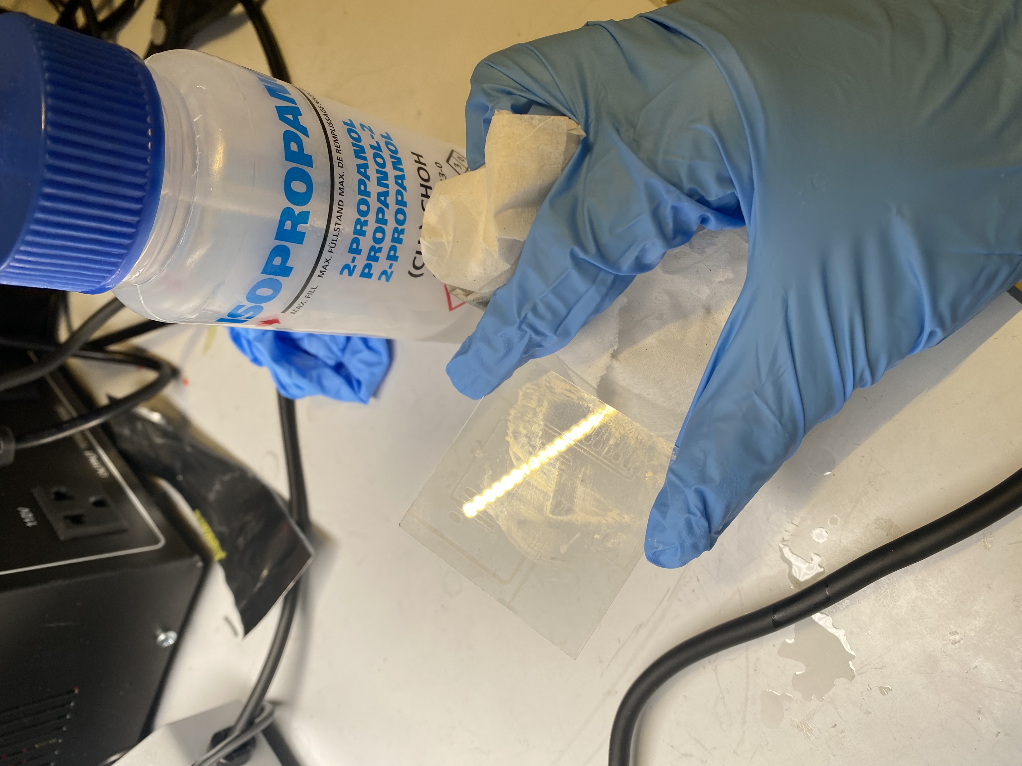
Cleaning up
This process was too frustrating that I often fell down to the floor after finding out there were bridges between the pads... I spent maybe more than 3 hours just to put parts on the glasses.
PC: Skye
PC: Skye
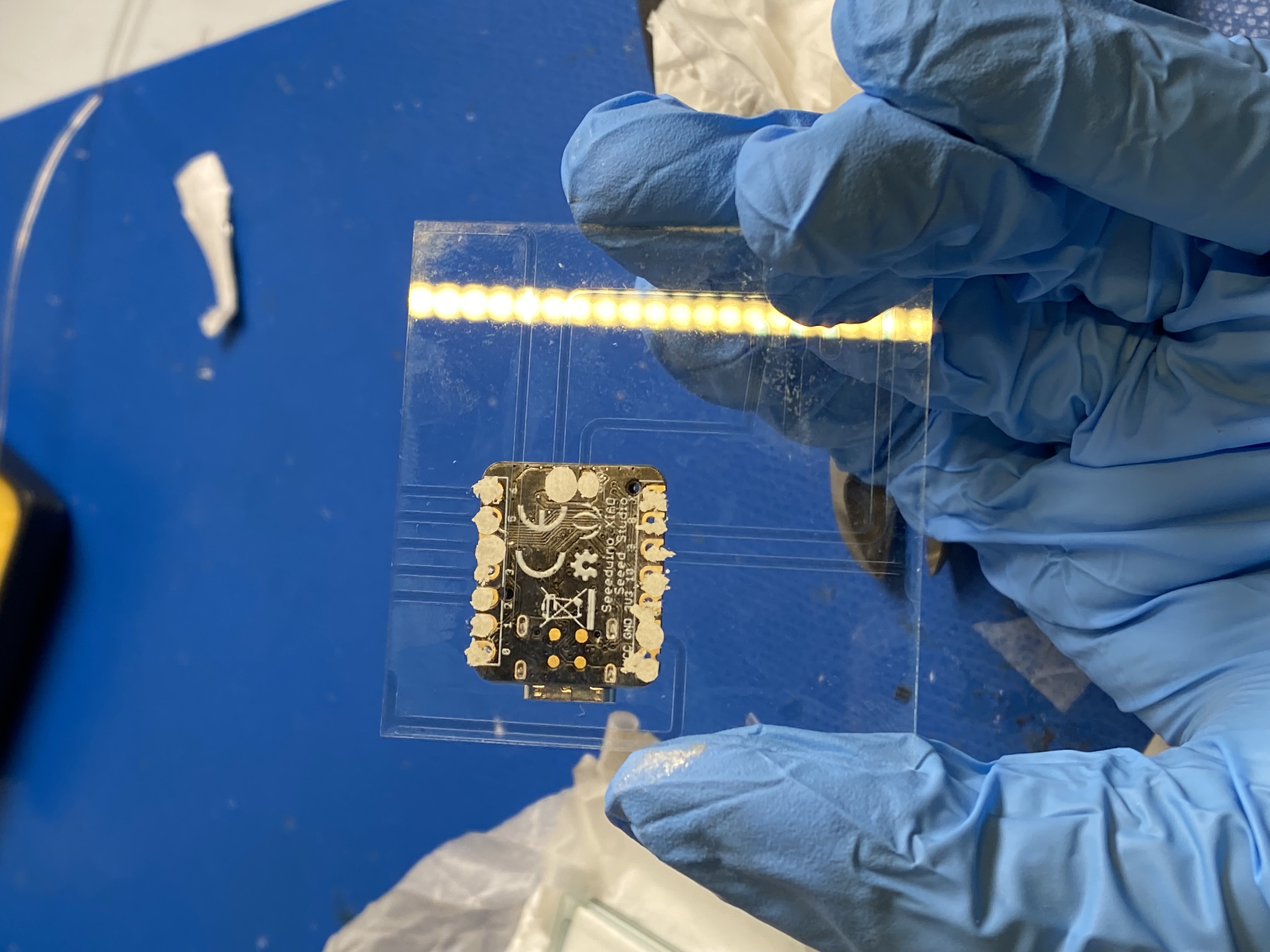
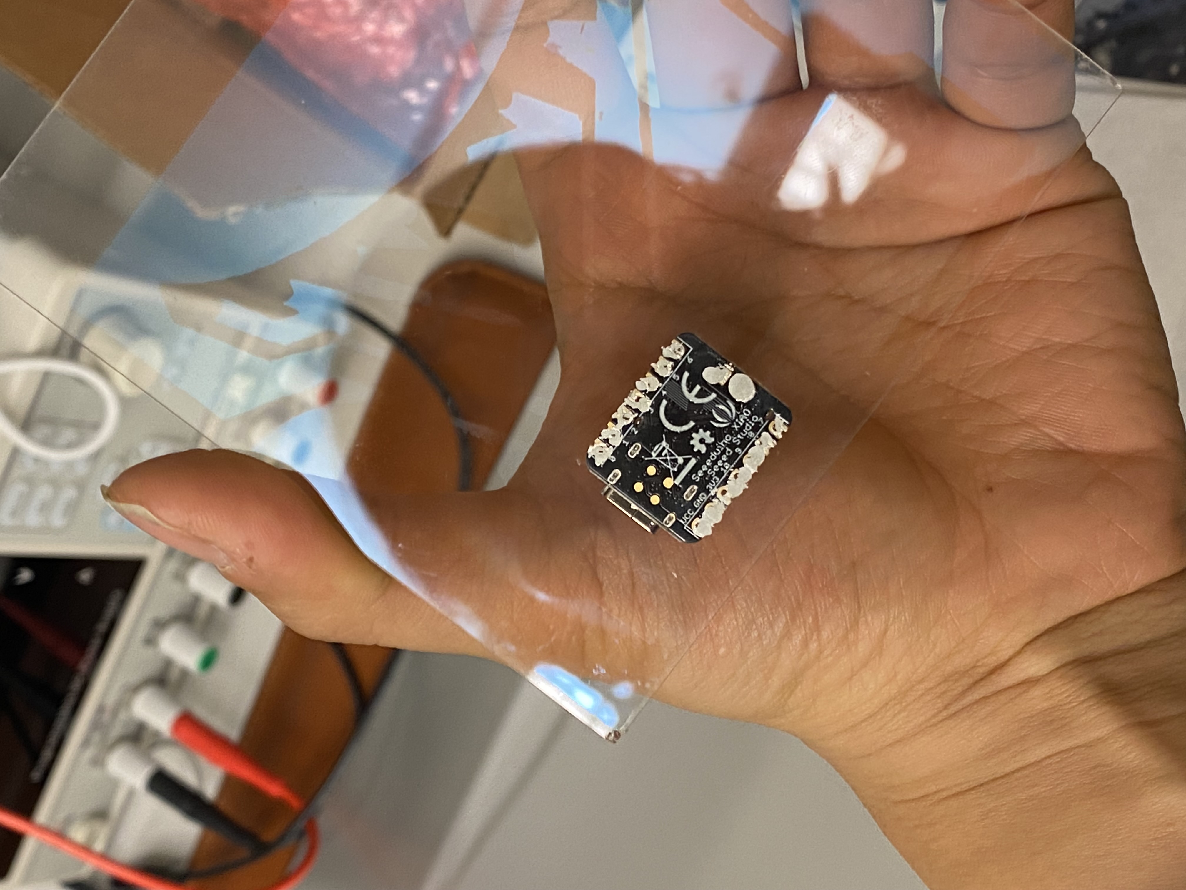
Re applied the silver epoxy and attached Xiao SMD board
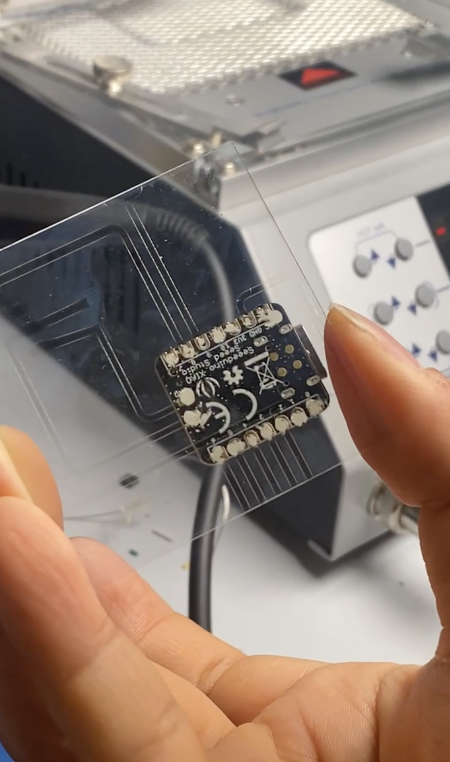
Will it work?
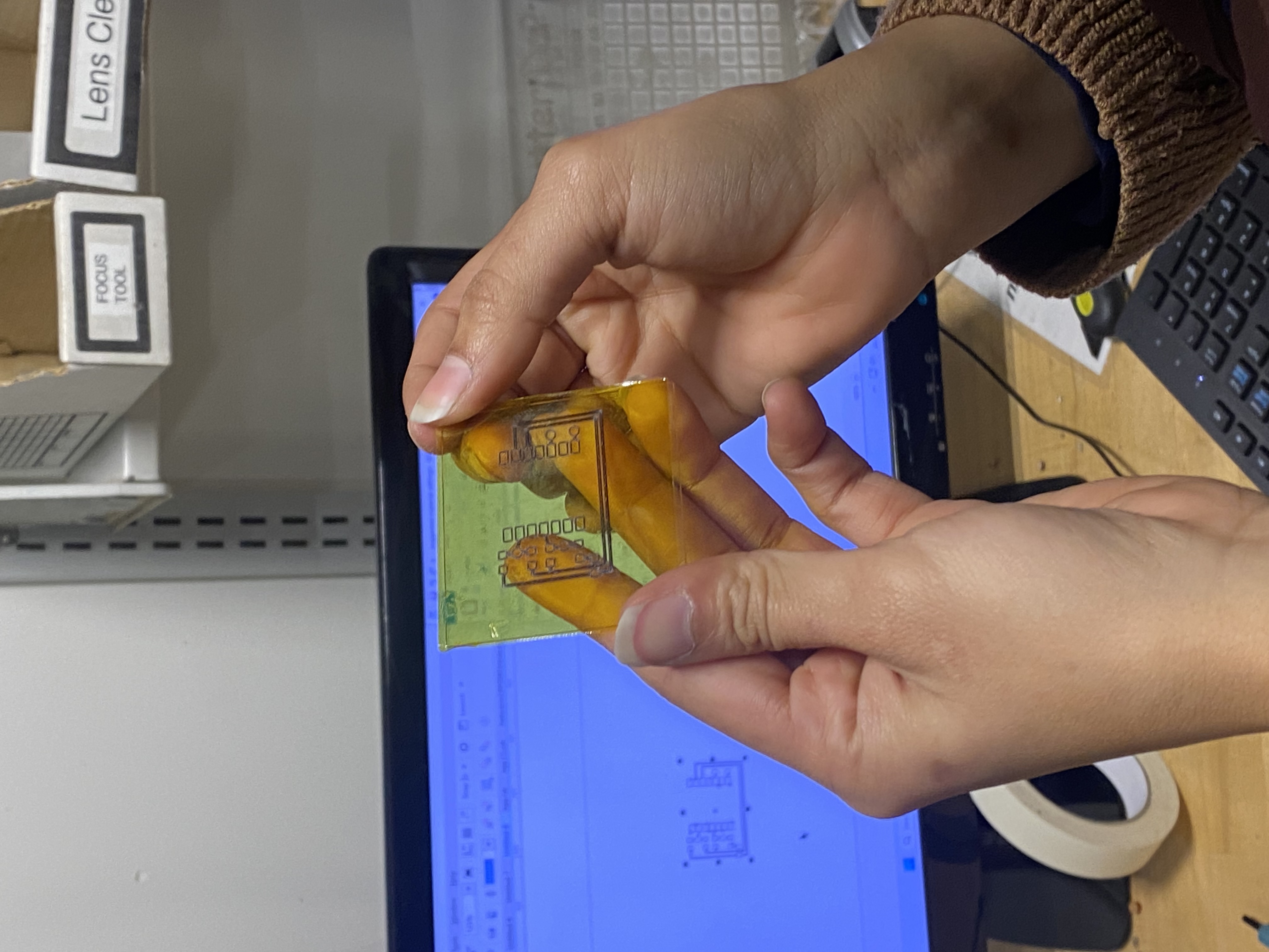
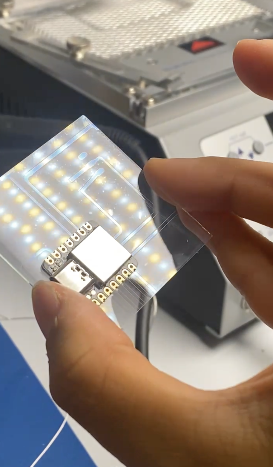
It works!


What if we could give a smile to someone with 10 LEDs?
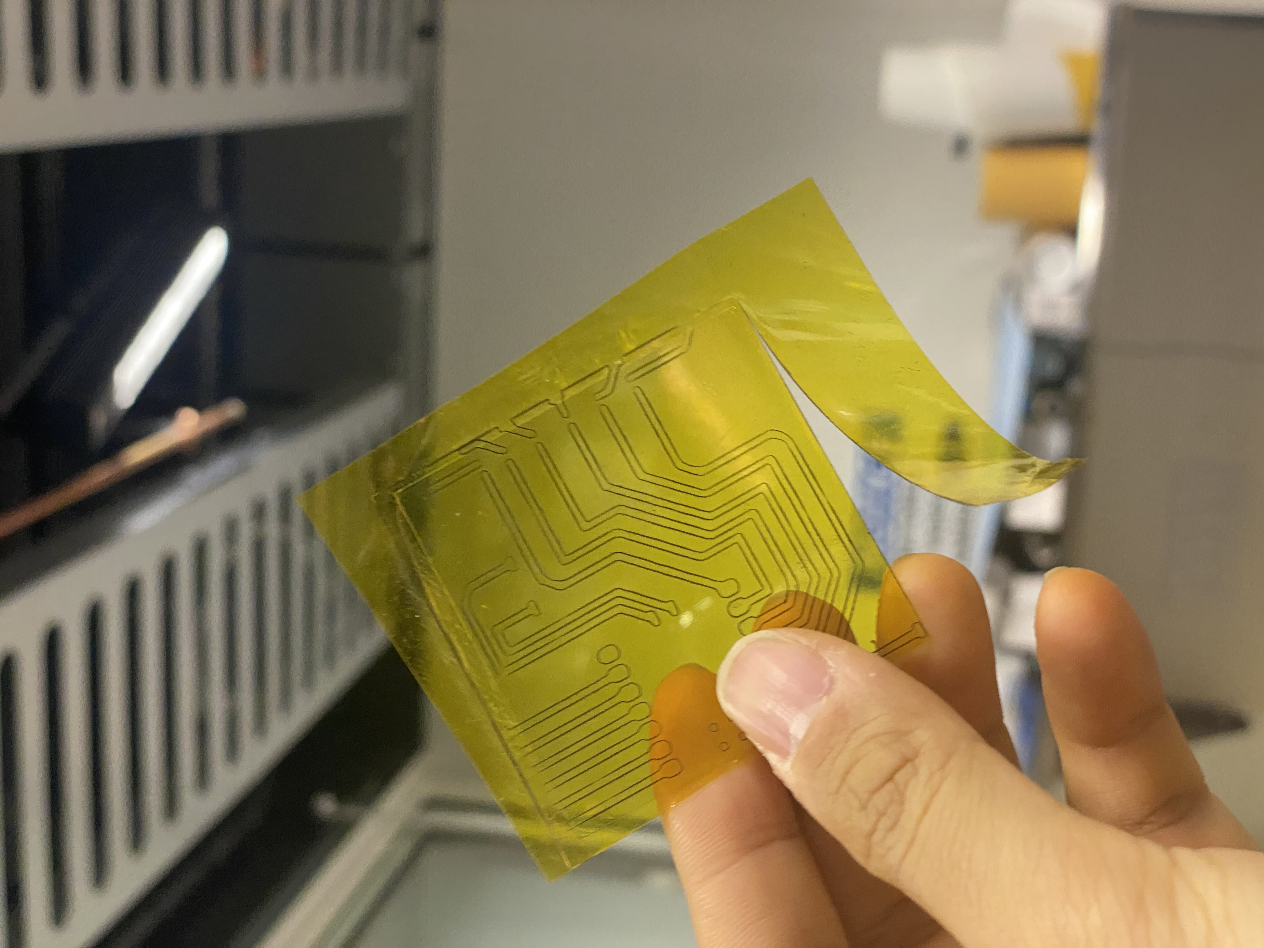
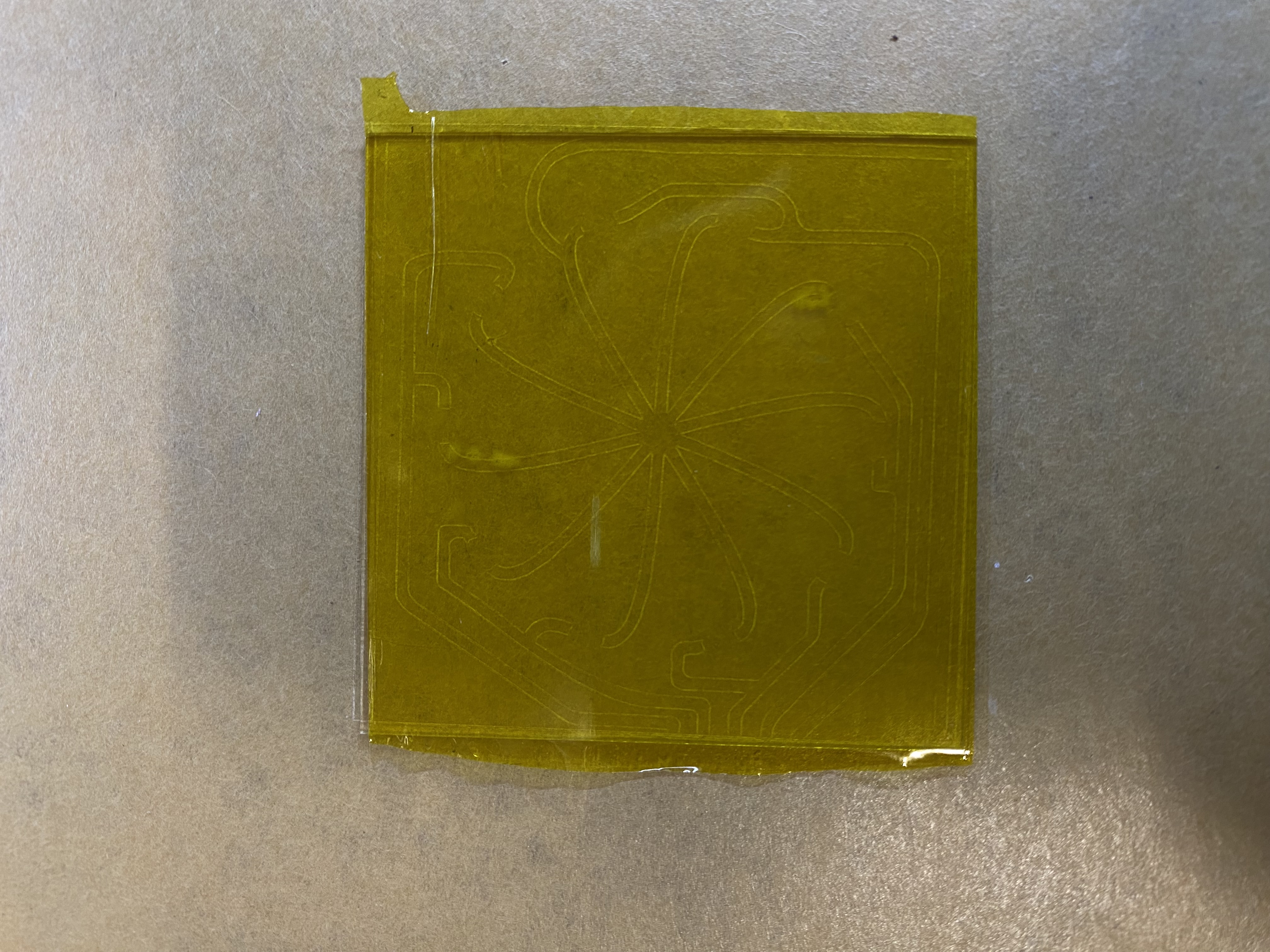
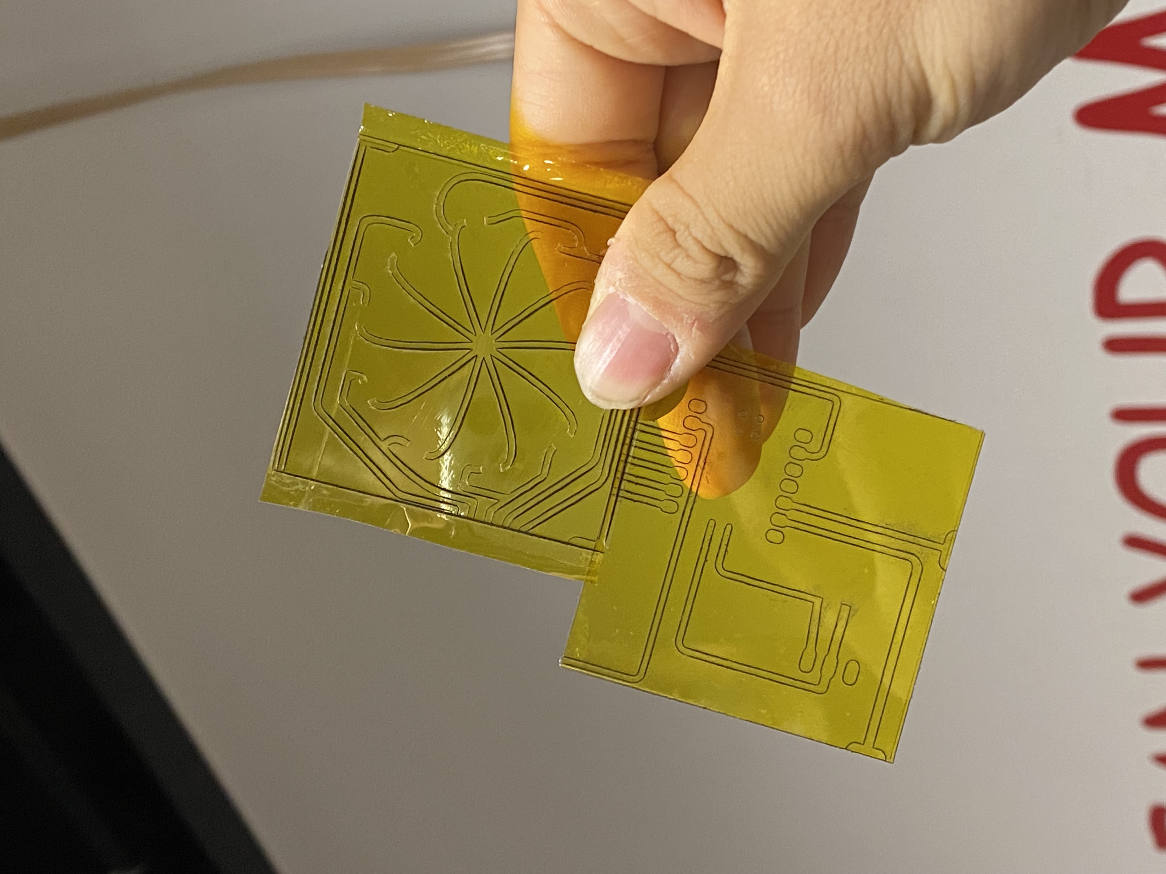
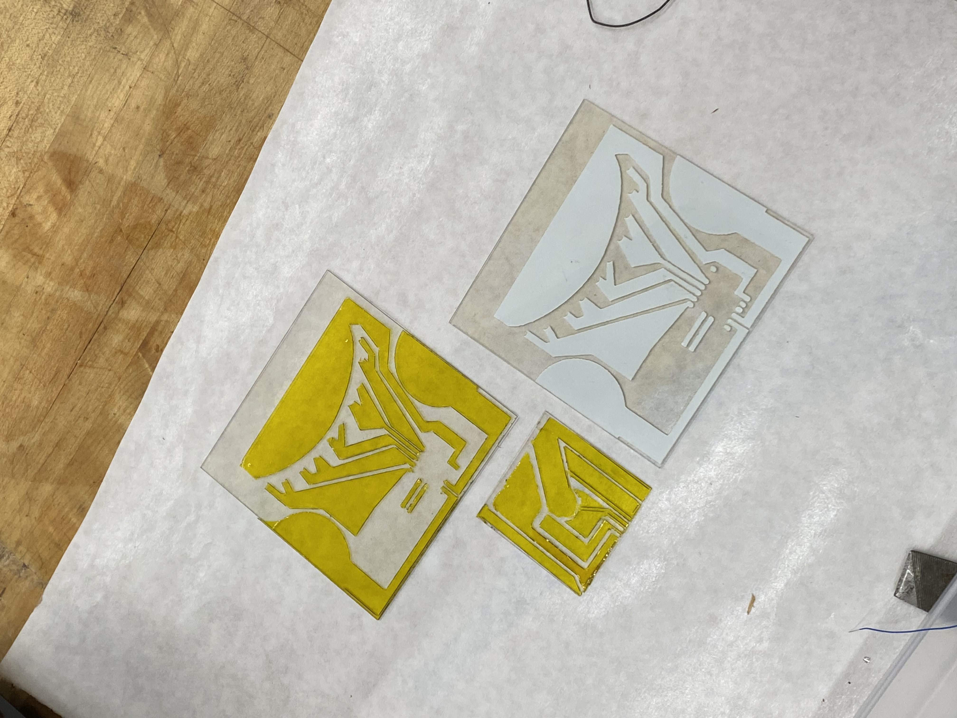
Started to test with wider sampels (100*100mm)
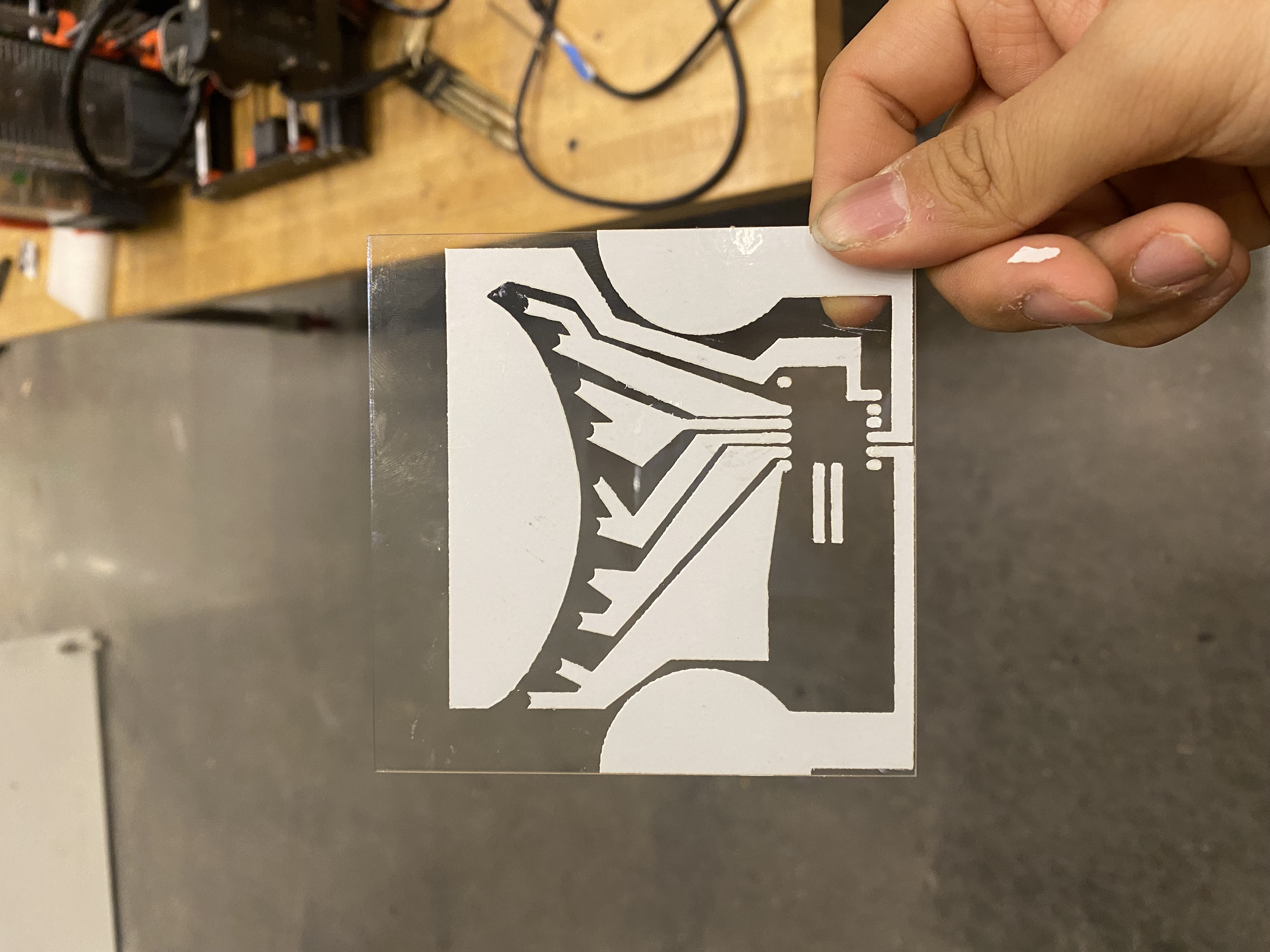
This design is for the smile with 10LEDs
and some others

Testing the conductivity
Applying silver epoxy
 Failed again
Testing LED
Attatched with Super glue + Silver epoxy and testing the LED

100mm*100mm samples didn’t work with Xiao, but I want to explore more with transparency as material

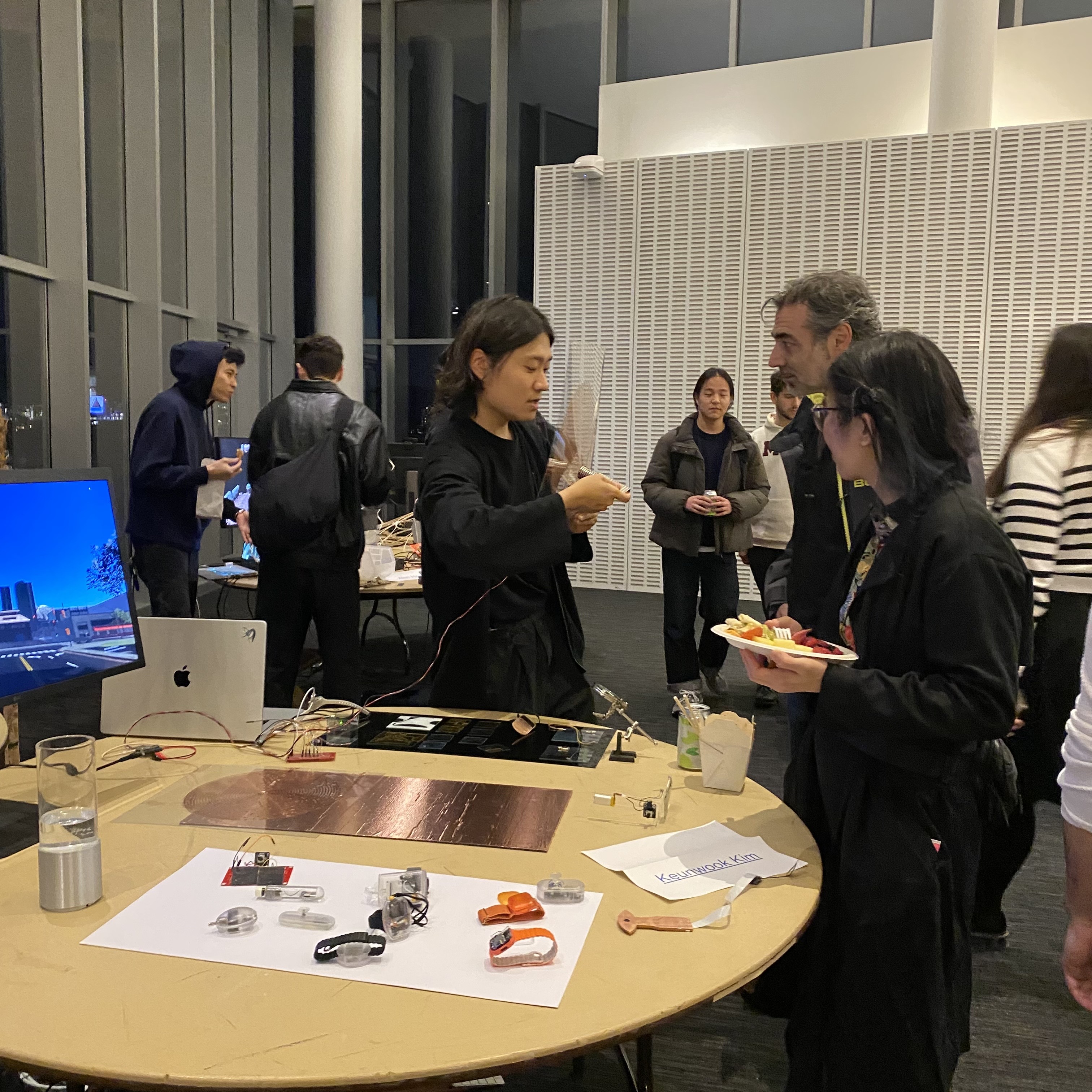
Final presentation Open House